Photoreceiver Characteristics

Photoreceivers are based on the same types of semiconductor photodiodes used for power sensors (see Photodiode Sensor Physics) and camera-based beam profiling (see Laser Beam Profile Measurement). Since these applications are mainly focused on steady-state (quasi-CW) optical response or, for a pulsed source, the time-integrated response, the actual temporal response of the optical signal is not critical. However, many applications require the monitoring of rapid events and therefore, high-speed optical detection is necessary. The characteristics of such high-speed photoreceivers as well as their associated applications are the subjects of this section. Photoreceivers focused on sensitive detection of optical signals at low-light levels or those that exhibit small differential changes are also addressed.

Since photoreceivers are semiconductor photodiodes, they possess the same intrinsic advantages described in Photodiode Sensor Physics e.g., large detectivities and very wide dynamic ranges. They also share many common parameters that must be considered when selecting a detector for any application. These include responsivity, spectral sensitivity, linearity, power handling, bias voltage, and power consumption. However, due to the nature of the specific applications for photoreceivers, there are unique characteristics as well. The attributes discussed in this section include rise time and bandwidth, methods for noise level reduction, as well as detector gain and active area.

Response Time

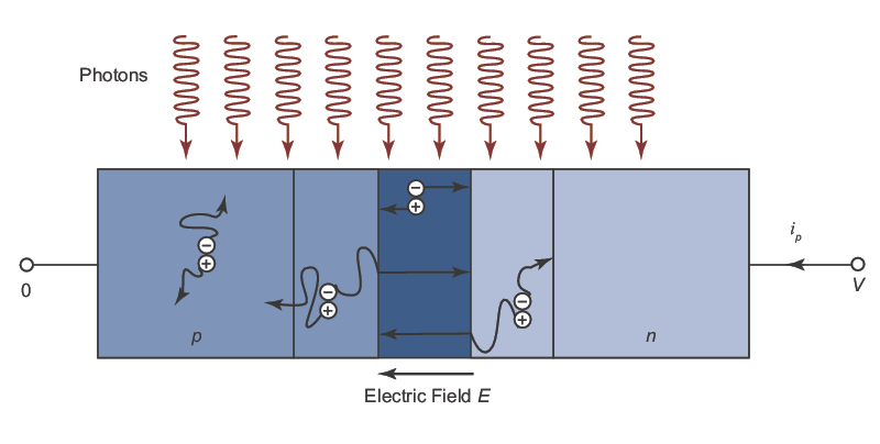
The conversion of photons to electrons is very rapid in photodiodes, which enables them to follow fast changing radiation levels. To understand this response time, it is instructive to revisit the operation of a reversed bias p-n junction (shown in Figure 1) that makes up a photodiode. Electron-hole pairs that are generated in the depletion region experience a strong electric field that causes them to rapidly drift in opposite directions. Charge carriers generated near the depletion layer can end up there following random diffusion and contribute to the external electric current. Carriers generated farther away from the depletion layer are highly likely to recombine and therefore not contribute to the current. The overall response time for current generation depends on the transit time it takes for carriers to drift across the depletion layer as well as the time for carriers to diffuse into this region. Diffusion is a relatively slow process compared to drift and so modifications to the p-n junction are often implemented to reduce diffusion (see Types of Photoreceivers).
The operation of a reversed bias p-n junction of a photodiode when irradiated by incident photons
Figure 1. The operation of a reversed bias p-n junction of a photodiode when irradiated by incident photons. Drift of the carriers occurs in the depletion layer (central dark blue region) while diffusion primarily occurs just outside this region.
The p-n junction of the photodiode is effectively a capacitor with capacitance C. When the photodiode is connected to a circuit with a load resistance of R (typically 50 Ω), the combination of resistance and capacitance effectively integrates the current. This lengthens the response time by a value known as the RC time constant. Therefore, the overall response time of a photodiode depends on the transit and diffusion times as well as the RC time constant. The benefits of operating under reverse bias for a photodiode power sensor were stated as greater light collection and a larger quantum yield. However, reverse bias operation also offers advantages in terms of reducing response time. The bias creates a strong electric field in the junction that increases carrier drift velocity leading to a reduced transit time. Also, the increased depletion width reduces the junction capacitance and the associated RC time constant. These benefits in terms of reduced response time are why most high-speed photoreceivers operate in reverse bias.

Rise Time and Bandwidth

For measurements in the time domain, the response time of a photoreceiver is quantified by its impulse response. This is essentially the shortest pulse one could expect to see from the detector and is often quantified in terms of the FWHM of the pulse in the time domain. More commonly, the parameter specified for a photoreceiver is the rise time, which is the integral of the impulse response. Figure 2 shows an example of a high-speed photoreceiver’s impulse response with a corresponding sub-20 ps rise time. Rise time is the appropriate parameter to consider in digital communications systems where bit streams are comprised of an endless series of rising and falling edges. Generally, the rise time of a detector should be at least three times shorter than the rise time you expect to measure. Sometimes, it is necessary to know the required frequency bandwidth for time-domain measurements. A good rule of thumb is to use a detection 3-dB frequency bandwidth (the frequency at which the power falls off to 50% of the value at DC) greater than 0.44/., where . is FWHM of the impulse response.
Impulse response of high-speed photoreceiver measured with 18.5 ps rise time
Figure 2. Impulse response of high-speed photoreceiver measured with 18.5 ps rise time (left, top) and a 3-dB power bandwidth of 20 GHz (left, bottom). Comparison between an idealized detector’s power bandwidth and voltage bandwidth (right).
For measurements in the frequency domain, such as laser heterodyning or optical modulation experiments, the photoreceiver should have a flat response out to the highest frequency of interest. This is typically quantified in terms of the 3-dB frequency bandwidth. The high-speed photoreceiver discussed above has a frequency bandwidth of 20 GHz as shown in Figure 2. There are many terms used to describe the bandwidth of a photoreceiver, which can lead to confusion when making detector comparisons. The “power bandwidth” (also known as the “electrical bandwidth”) is the 3-dB point of the power spectrum and is the most common value reported. The “voltage bandwidth” (sometimes called the “optical bandwidth”), or the 3-dB point of the voltage spectrum, is offset to higher frequencies than the power bandwidth since power is proportional to the square of the voltage. As shown in Figure 2, this implies that the 3-dB voltage bandwidth is always greater than the 3-dB power bandwidth for the same photoreceiver.

Noise Reduction

The sources of noise in photoreceivers and the associated parameters describing noise characteristics were discussed in Radiometric Measurement. Here, methods to minimize the photoreceiver noise are addressed. These approaches essentially involve choosing the best match of detector response to signal characteristics. The regimes in which detector response can be optimized include time, wavelength, bandwidth, and active area. When measuring pulsed optical signals, gated averagers or integrators are used to improve the SNR. These devices take their names from the gates, boxes, or windows that are used to define the times during which the electronics acquire the signal (see Figure 3). During these gated times, the SNR is improved since noise contributions which would normally accumulate during the non-gated times are absent. If the process is repeated N times, the SNR will improve by a factor of N1/2 for most types of noise. The spectral sensitivity of the photoreceiver must cover the wavelength range of the signal. However, if the detector’s wavelength sensitivity range exceeds that of the signal, any radiation outside of the signal range will contribute to noise. The use of a bandpass filter (see Optical Filter Design) to narrow the range of wavelengths seen by the detector can reduce this undesired noise. The level of noise reduction depends on how optimal the spectral overlap is between the filter and the signal, as shown in Figure 3.
Introduction of gated windows to reduce noise in the time domain
Figure 3. Introduction of gated windows to reduce noise in the time domain (top). Matching of detector responsivity to signal to reduce noise in the spectral domain (bottom) with efficiency increasing from left to right.
Frequency bandwidth can also be adjusted to reduce noise. AC detection methods use electronic and digital filters to match the detection bandwidth to the signal’s frequency spectrum. The signal is discriminated from the noise contribution, which will have its power spread over a different and wider band of frequencies. The signal may have its own natural modulation frequency around which the filter can be centered or a known modulation can be applied to the signal. This can be accomplished through optical modulation using a chopper or by electronic modulation. Then, an AC-coupled amplifier with a narrow band filter centered on the modulation frequency helps significantly increase the SNR. More sophisticated approaches involve the use of lock-in techniques where the amplifier actively tracks the modulator frequency, allowing much narrower band filtering to be used.

Active Area

The benefit of a large area photodetector in the context of power measurements was discussed in Radiometric Measurement. Similarly, alignment of a large laser beam into a photoreceiver is made significantly easier if the detector has an active area ranging from several mm2 to cm2. However, since noise is proportional to the area of a detector, such large-area photoreceivers are noisy. Reduction of the active area of a photoreceiver is therefore often desired for improved SNR. This is typically accomplished using optical fibers to deliver the light directly to the active area. The active area is essentially matched in size to the core of the fiber, which have diameters of 50-60 µm for multimode fibers and less than 10 µm for single-mode fibers. Reducing the active area also increases response speed. This is a by-product of the reduced junction capacitance, which in turn reduces the response time. Due to the benefits of reduced noise and response time, many high-speed photoreceivers are fiber-coupled.

Gain

As discussed in Photodiode Sensor Physics, a photodiode has a high quantum yield or probability that an incident photon will produce a detectable charge carrier pair. These carriers then produce a single charge in the photoreceiver circuit. In other words, photodiodes do not exhibit intrinsic gain like some other detectors (see description of low-light photoreceivers below). However, a photoreceiver with an electronic amplifier will exhibit gain defined as the average number of circuit electrons generated per photocarrier pair. A more commonly reported parameter for a photoreceiver is the maximum conversion gain which describes the resulting output voltage (V) for a given input optical power (W). Given in V/W, the conversion gain is the product of the photodetector’s responsivity, the amplifier’s gain, and the input impedance. For an unamplified photodetector, the conversion gain is the product of the photodetector’s responsivity and the load impedance. Photoreceivers also possess a fixed gain-bandwidth product such that an increase in gain results in a decrease of the bandwidth, and vice versa. This trade-off between sensitivity and frequency response is associated with the time required for the gain process to take place.

MKS Semiconductor Handbook Cover

For additional insights into photonics topics like this, download our free MKS Instruments Handbook: Principles & Applications in Photonics Technologies

Request a Handbook