Flat Panel Display Manufacturing
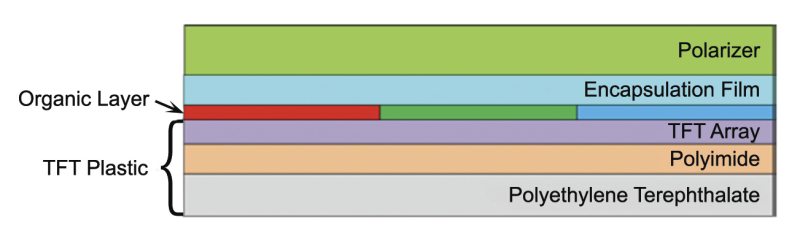
As the flat panel display market moves from liquid crystal displays (LCDs) to organic light emitting diode (OLED) display technology, laser patterning and cutting of heterogeneous materials (comprised of multiple organic material films) with high quality and accuracy is needed. Within OLED technology, substrate materials are moving from glass to flexible plastics to create lighter, thinner and more durable displays. Flexible OLED structures consist of a multilayer stack of functional materials deposited on heat sensitive plastic films such as PI and polyethylene terephthalate (PET) as shown in Figure 1. The sensitive thermal and optical properties of these films make these stacks difficult to machine using conventional laser sources.
Fs lasers are capable of machining plastic materials with a minimal HAZ and precise control of the material removal. Although the processing quality achieved meets industrial demands, processing speeds need to be improved to satisfy the industrial user. To process parts quickly and cost-effectively, a fs laser system with high average power is required. Additionally, the laser system must be robust and stable to sustain the demands of the production floor.
ClearShape Industrial Laser Cutting Process
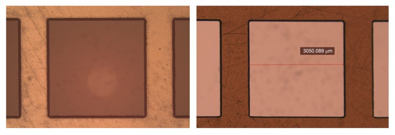
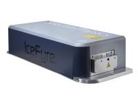
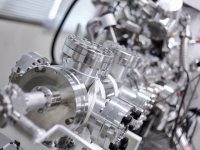
The Spirit® 1030-100 laser is a high-power industrial fs laser used in high-precision industrial manufacturing. This laser offers impressive versatility and performance, enabling a variety of applications. High average power (> 100 W) and high pulse energy (> 100 μJ) at a wavelength of 1030 nm, combined with a high PRF (up to 10 MHz) and short pulse duration (< 400 fs), pushes fs micromachining applications to desirable throughput levels with low cost-of-ownership. The user-configurable burst mode further enables processing with increased ablation efficiency and thus increases throughput and quality for certain materials. Additionally, the integrated SHG module offers an output power of > 50 W at a wavelength of 515 nm, which is useful in machining stacks of materials with different optical properties. The Spirit 1030-100-SHG laser system operating at wavelengths of 515 and 1030 nm has been used for cutting 75 μm thick ribbons of PI and PET plastics, typically used for flexible OLED displays. Figure 2 shows microscope images of PI and PET plastics machined using the Spirit 1030-100-SHG laser. Cutting speeds exceeding 1 m/s for both plastics were achieved when operating the laser at 100 W average power at 1030 nm. It was also possible to achieve high machining quality with minimal thermal damage (HAZ < 50 μm). The demonstrated cutting speed and quality meets the requirements of OLED display manufacturers.
Process Challenges in OLED
Flat panel displays use different backplane technologies. Small and medium OLEDs for mobile phones use a low temperature polysilicon (LTPS) backplane which is created by laser annealing amorphous silicon (a-Si). OLED TVs use a metal oxide backplane. Both backplanes use deposited thin films which must be highly uniform and contamination free to maximize electrical performance. The OLEDs are evaporated or deposited and encapsulated to reduce degradation caused by water vapor and oxygen exposure. Encapsulation uses either strengthened glass or thin films, depending on whether the OLED is rigid or flexible. Dissimilarity of materials within the rigid and flexible stacks make cutting and singulation of individual display devices a challenge. The highly complex nature of this process can induce defects, decreasing throughput and yield.
Challenges in OLED manufacturing include:
- Contamination-free thin films
- Precise cutting with minimal damage to surrounding areas or structures
- Low throughput
- Yield
OLED Manufacturing Solutions
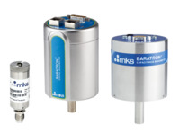
Direct Pressure Measurement
The LTPS backplane conducts electric current to the OLEDs so light is emitted. This layer is created by vacuum deposition of a-Si either directly on strengthened glass or onto a polyimide layer attached to a glass carrier. The thin film is then laser annealed to create the crystalline LTPS structure. To ensure the correct composition and uniformity of the a-Si thin film, it is important to directly measure pressure within the deposition chamber. Direct Pressure Measurement devices from MKS operate in situ, with low pressure measurement drift and EtherCAT® communication. This makes it highly reliable and quick to communicate with the overall system ensuring correct composition and uniformity of a-Si thin films.
Ozonated Water Delivery
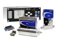
Surface cleanliness prior to a-Si deposition is important to ensure contaminates don’t negatively impact the thin film electrical properties. Our Ozonated Water Delivery Systems provide pure, high flow and high concentration ozone that rapidly oxidizes organics including metals and particles. Exposure to ozone at this stage of the manufacturing process improves the grain size and uniformity of the LTPS thin film layer improving the backplane’s electrical characteristics. It is important to clean with ozonated water after laser annealing to ensure no new contaminates have been deposited on the surface prior to the RGB evaporation step.
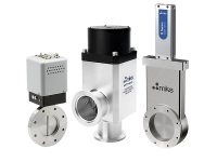
Remote Plasma Sources
Routine cleaning of the vacuum deposition chamber using our Remote Plasma Source (RPS) systems reduces potential film contamination by removing chamber wall contaminates. The RPS delivers productive NF3 over a broad pressure range from 5-40 Torr and with low volume up to 50 slm. This results in increased speed of chamber clean and equipment uptime. To shorten chamber cleaning time, our Non-dispersive Infrared (NDIR) Chamber Clean Endpoint System senses SiF4 down to 1 ppm, optimizing chamber clean time by measuring process byproducts.
Pixel Hole Machining Lasers
RGB pixels are evaporated on the LTPS backplane surface using an invar Fine Metal Mask (FMM). As OLED manufacturers push for >1000 pixels per inch (PPI) to support VR, a new way to create a fine metal mask with increased pixel density and feature accuracy is necessary. Our Micromachining Lasers, with picosecond or femtosecond pulses and small, focused beam widths, create completely vertical pixel holes with no material buildup that could negatively impact feature geometry. Ultrashort pulses reduce excess heat buildup providing a minimal heat affected zone. This reduces mask warp and ensures all pixel holes maintain their shape. The laser’s high output power, high beam quality and narrow bandwidth supports highly uniform beam splitting for parallel machining and increased throughput.
Glass and Film Cutting Lasers
Our industrial femtosecond and picosecond display manufacturing lasers are excellent for glass and film cutting. For cover glass and rigid OLED, they provide flexible pulse and burst control with precision, resulting in a micro-crack, chip-free edge, making the glass stronger and less likely to break if dropped. This reduces the need for post-cut polishing, increasing throughput by reducing the number of manufacturing process steps. For flexible OLEDs, Spectra-Physics lasers with short pulse widths create a minimal heat affected zone and provide a clean cut through layers of dissimilar materials including various thin films, PET, and adhesives. Increased throughput is achieved from higher output power that speeds up the cutting process. The narrow kerf or cut and the low heat affected zone means more parts can be cut out of the same material.
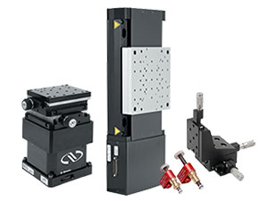
Beam Delivery Optics
Our high performance optics have various coatings that are optimized for different wavelengths, enabling tight beam delivery - important for tight radius corner cuts for both glass and film cutting. Combined with our linear stages that have high, stable velocity with on-off laser synchronization, MKS is uniquely positioned to provide a variety of solutions that enable precise radius cutting at the micron level for both film and glass.
Flat Panel Display Manufacturing Products
For additional insights into photonics topics like this, download our free MKS Instruments Handbook: Principles & Applications in Photonics Technologies
Request a Handbook