PCB Manufacturing
Lasers are routinely used in a variety of PCB manufacturing processes including via drilling, depaneling, profiling (cutting), laser direct imaging (LDI), repair, trimming, and marking. Laser technology being a non-contact process completely eliminates mechanical stress on the material. Burr formation and micro-cracking in material are also avoided. The tighter focus achievable with UV lasers can controllably remove small volumes of material, reducing deposits of ejected material on the circuits. Precision micromachining achievable with UV lasers allows more circuits to fit on a single panel, increasing the net usable area. Moreover, UV wavelengths are absorbed by a variety of materials in PCBs, from copper to polyimide films, thus providing a onesolution-for-all-materials-and-processes kind of flexibility. For example, the high beam intensity achievable with tighter focus UV can remove copper, while lower beam intensity achieved by reducing laser power can cut dielectric material without damaging the bottom copper layer.
Cutting and Drilling of PCB Materials
One large and growing market for laser processing is PCB manufacturing. The market has traditionally used CO2 and excimer lasers but is increasingly moving towards UV DPSS lasers. The migration to UV DPSS laser technology is driven by several factors, including the need to machine smaller features with higher precision and density and the ability of UV wavelengths to process many types of materials with good quality. Furthermore, UV DPSS products available on the marketplace have experienced reduced cost and cost of ownership.
The Spectra-Physics Talon UV product family consists of industrial UV lasers with ns pulse widths. The Talon product family is highly versatile with a wide range of configurations in terms of power, energy, and pulse repetition frequency (PRF). For example, the 15 W UV Talon offers a high pulse energy of 300 μJ at a 50 kHz PRF for larger feature machining in thicker materials such as FR4-based rigid PCBs. On the other hand, the 20 W UV Talon has lower maximum pulse energy but maintains an elevated output power level at very high PRFs. These parameters are ideal for processing thinner materials with a tight beam focus and can enable high-speed, high-resolution machining.
As electronic devices shrink and improve in performance, the need for compact and thin flex-PCBs to which the electronic devices are mounted is growing rapidly. Flex-PCBs are typically made using layers of materials that have several to tens of .m thicknesses. Materials used include copper (Cu) foils, polyimide (PI) sheets, and adhesives that enable the creation of various laminates. A typical flex-PCB material is comprised of a 12 μm thick PI layer laminated between two Cu foils of similar thickness. In flex-PCB fabrication, laser processes may include blind- and thru-via drilling, straight-line and contoured cutting, as well as 2D patterning. Given the high power and high PRFs available from the Talon UV laser, MKS has been able to optimize various high-speed processes for use with flex PCB materials.
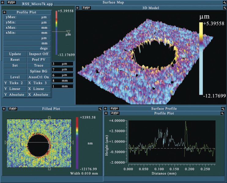
It is possible to achieve high quality cutting and drilling performance at high speeds by optimizing the scanning speed and PRF to achieve the proper spot overlap in the material. The Talon laser's high average power at high PRFs provides sufficient pulse energy to ablate Cu material up to several hundred kHz. Cu/PI/Cu laminates can be cut through with the Talon 355-20 laser at speeds exceeding 450 mm/sec while operating at 500 kHz. As shown in Figure 1, exceptional cutting quality is achieved with minimal burring and a small HAZ. The Talon UV laser has also been tested for high-speed percussion drilling of blind vias in a similar Cu/PI/Cu laminate material. In this case, the middle PI layer was twice as thick, at 25 μm. High-quality vias with sub-30 μm diameter openings were processed at very high PRFs to minimize the drilling time. With the Talon laser operating at 300 kHz, just twenty pulses were required for drilling each hole, which equates to a throughput of 15,000 holes per second. Thin PI films are also used extensively in flex-PCB manufacturing as coverlay materials to protect circuitry from harsh environments, similar to solder masks in thick PCB manufacturing. UV wavelengths are very effective for processing PI with high quality and precision due to the strong optical absorption by the material and subsequent photo-ablation. With commonly-used thicknesses of 12-25 μm, optimal cutting of these materials is achieved with a high PRF, lower energy laser source. The Talon laser is ideal for such requirements and a wide range of cutting speeds are possible with the various product offerings.
PCB Manufacturing Products


For additional insights into photonics topics like this, download our free MKS Instruments Handbook: Principles & Applications in Photonics Technologies
Request a Handbook