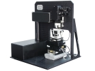
Our Laser µFAB™ Microfabrication Workstation is a table-top easy to use micromachining tool for various applied materials research fields. This device combines the flexibility and accessibility of a typical research grade experimental setup with the stability, reliability, and ease of operation of a fully developed industrial instrument. We also offer custom Industrial Laser Micromachining Solutions.
Micromachining workstation based on laser direct-writing
Perform additive, subtractive, and transformative processes
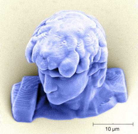
Complex and arbitrary three-dimensional microstructures are easily manufactured using the Laser µFAB™ and the proprietary material developed in the Technology and Applications Center. Preferable lasers to use for this application are the Spectra-Physics Mai-Tai and HighQ-2-SHG.
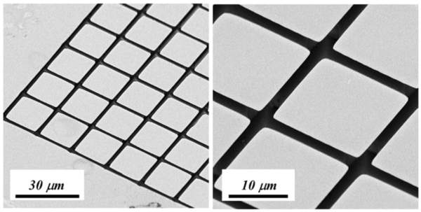
Clean Laser Ablation
When coupled to Spectra-Physics Spirit laser, the Laser µFAB™ can perform subtractive processes on many materials. Because of the laser short pulses and the workstation motion precision, accurate, precise, and clean two-dimensional patterns can be fabricated.
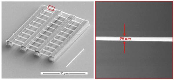
Achieve Feature Sizes Smaller Than 100 nm
By focusing the light with high NA microscope objective and by taking advantage of materials and optical nonlinearities, feature sizes smaller than the diffraction limit can be achieved using the Laser µFAB™.
Micromachining of Positive Photoresists
Positive photoresists are the most common materials used in photolithography to create microelectronics. The users of the Laser µFAB™ can now access the patterning of positive photoresists by means of laser femtosecond laser direct-writing.
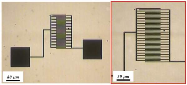
Laser Writing of Two-dimensional Metallic Patterns
The Laser µFAB™ is an excellent tool for driving spatially controlled deposition of metals. Patterns covering areas as large as squared centimeters can be written with features sizes on the order of microns. The Laser µFAB permits direct writing of several metals (Ag, Au, Cu, Al) with high efficiency. Laser assisted deposition of metals is achieved using easy-to-prepare gel matrices in which nanoparticles of the metal of interest are imbedded with stabilizing agents.
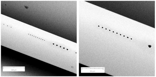
Drilling Holes on Optical fibers
The Laser µFAB™ has the accuracy and repeatability that are indispensable for precise microfabrication of optical fiber. By using the fundamental emission of Spectra-Physics Spirit laser (1040 nm) as the excitation source, drilling of holes on the surface of stripped optical fibers is possible. Modulating the laser exposure time, permits the creation of holes with different diameters and depths.
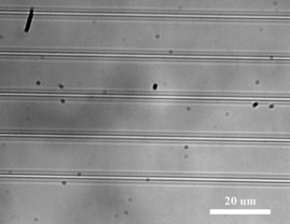
Waveguide Writing
When performing femtosecond laser direct writing in glass, permanent changes due to structural or phase modifications occur in regions of the substrate that were irradiated. These modifications are highly localized because they results from the laser-induced optical breakdown which develops there where the highest electrical field is generated (the volume of the focused laser beam). For several glasses it is possible to find the proper writing conditions so to produce a smooth modification, thus creating optical waveguides.
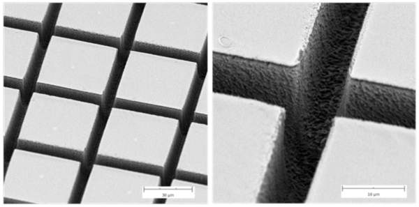
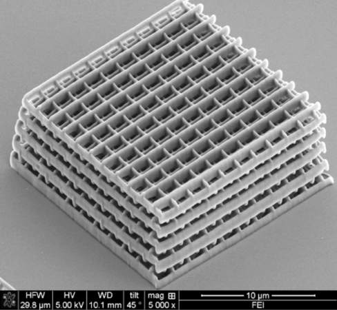
Three-dimensional Photonic Crystals
Photonic crystals are structures that present periodic alternation of materials with different indices of refraction. The most common photonic crystal is the one with a log–pile geometry that consists of layers of parallel rods in which the rod orientation in each layer is perpendicular to that of the adjoining layers. Photonic crystals have the interesting property of forbidding the propagation of certain modes of the electromagnetic spectrum. It turns out that this photonic band gap phenomenon occurs at wavelengths corresponding approximately to the distance between the rods. Thus, TPP is the preferred technique for the fabrication of photonic crystals that operate in the visible and near-IR regions of the spectrum.
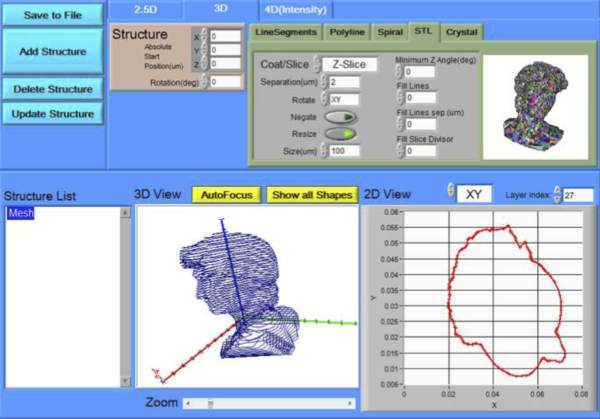
Microfabrication Software Included
Software for advanced laser microfabrication is included in the Laser µFAB™. By using a simple and intuitive GUI, users have full access to motion and laser controls. Furthermore, ad-hoc structure files can be generated within the software. Complex 2D and 3D design can be imported using DXF and STL extensions.
Bulk Micromachining of Transparent Materials
Fabrication of microfluidics networks in transparent materials is fundamental for the realization of complex lab-on-a-chip solutions. With the Laser µFAB™, users can form channels in the bulk of materials such as fused silica through femtosecond laser irradiation followed by chemical etching.
In order to provide better service and products, please provide the following brief information.
Password Reset
Enter your email address below to reset your account password.
Password Reset
Email Verification Required
Cart Items Updated
Remove Product
Remove this product from your comparison list?
Check Order Status
Provide an order number and postal code to check the status of an order or download an invoice for an order that has shipped. Login to view your complete order history.
Sign In Required
To access this and other valuable technical resources, please sign in or register for a new online account.
 Over 8,000 products in-stock! & FREE 2-Day shipping on all web orders!* Learn More FREE T-Shirt with orders $250+ Details
 Ultra-High Velocity