Sorry, this family of products is no longer available.

µFAB-L Micromachining Workstation
µFAB-L Micromachining Workstation
Newport’s µFAB-L workstation is a table-top easy to use micromachining tool for various applied materials research fields. This device employs high performance galvanometer scanners for fast laser writing and a XYZ stage assembly for sample positioning. The included software allows importing several types of CAD files and permits large areas microfabrication by stitching galvos and stages motion.
- Micromachining workstation for fast writing of large areas
- Ideal for fast prototyping of parts in advanced R&D laboratories
- Micromachining with minimal heat affected zone when used with fs lasers
- Can be integrated with CW, ns, ps, and fs lasers
- Machine hard to process materials such glass, ceramics, alloys, and composite materials
- Minimum feature size of 10 µm See All Features
Specifications
- Wavelength Range350 to 1100 nm
- Beam Diameter (1/e2)5 mm
- Attenuation RangeOD0 to OD4 (Computer Controlled)
- Travel Range X, Y, Z150 mm, 150 mm, 13 mm
- Maximum Speed X, Y, Z50 mm/s, 50 mm/s, 1 mm/s
- Minimum Incremental Motion X, Y, Z0.10 µm, 0.10 µm, 0.05 µm
- Galvanometric Mirror Marking Speed2 m/s
- Galvanometric Mirror Repeatability< 2 µrad
- Angular Resolution2.8 µrad for angle range of +/- 0.36 rad
- Weight86 kg
- Dimensions762 x 762 x 762 mm
Features
Laser Ablation
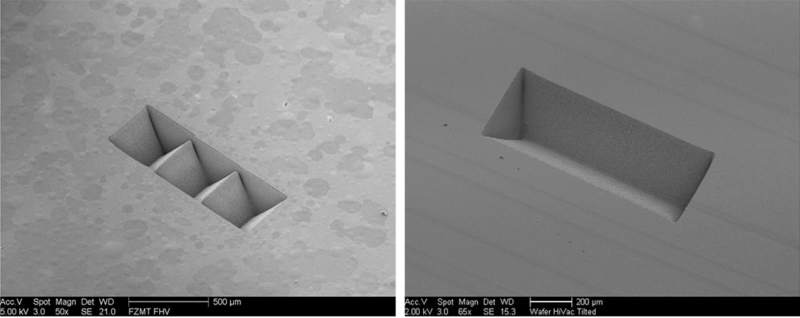
The ability to remove material with high spatial resolution and in a tool-less fashion is a prerogative of machining by laser direct writing. Several applications are performed using laser ablation such as nano-materials production, realization of MEMS components, and deposition of thin dielectrics films. Depending on the laser employed, customers using the mFAB-L will be able to cut, drill, and remove material from substrates as diverse as soft biological tissues and hard dielectrics. The images below show an example of micromachining by ablation of borosilicate glass using Spectra-Physics Spirit laser.
Surface Texturing
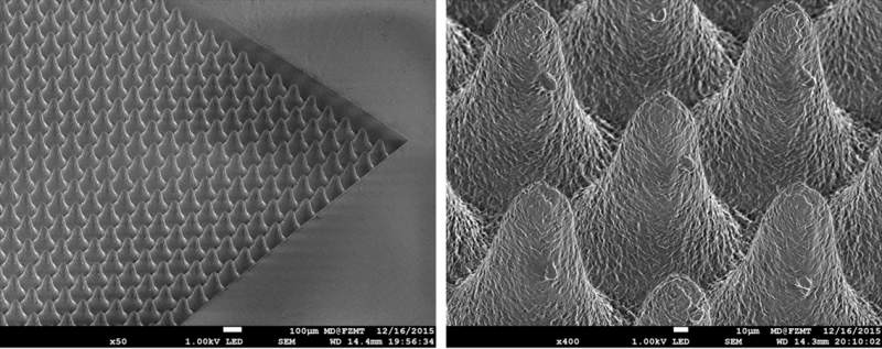
Texturing surfaces with micro- and nano-structures by laser direct writing has emerged in the last fifteen years as an excellent and efficient manufacturing method for delivering materials with significant improvements in wettability and wear resistance. Moreover, optical properties of materials can be tuned by introducing a rationally designed surface roughness. Finding the right experimental conditions to create the desired surface effect can be time consuming. When using the mFAB-L with Spectra-Physics Spirit laser, the user will have easy access to all the experimental parameters required for the realization of these structures. An example of surface structuring is shown where conical shaped microstructures were obtained in polypropylene by laser direct writing, rendering the laser written surface hydrophobic.
Thin Film Scribing
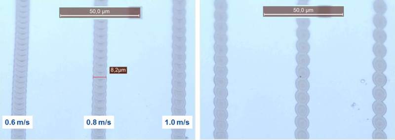
Deposition of thin films is an essential step in the manufacturing of several devices from solar cells to flat screen displays. For the realization of these devices, another key process is the selective removal of thin films with good spatial control. Thin film laser scribing is the best choice when high precision and contamination control are required. The uFAB-L is an attractive solution for thin film scribing since it delivers a perfect combination of accuracy with writing speed. An example of thin film scribing is shown in the following images where a 200 nm thick layer of ITO was selectively removed from a polyethylene terephthalate.
Technical Articles
The µFAB-L workstation has been featured in the following technical articles.
Photonics.com
-
Two-Photon Polymerization: Additive Manufacturing From the Inside Out
-
Laser Microfabrication Techniques Move Rapid Prototyping to the Mainstream
Application Focus