Optical Power Measurement Basics
Photodiode Optical Sensor Basics
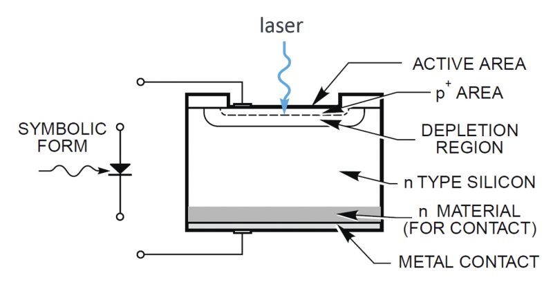
When a photon hits the photodiode material, it may generate an electron-hole pair depending on the quantum efficiency of the device. Quantum efficiency is dependent on many factors, but in general if the energy of the photon, E = hv, is greater than the energy gap of the device, these photons will be absorbed very near the surface where the recombination rate is high and will contribute to the photocurrent. It is the quantum efficiency that is responsible for the wavelength dependency of the photodiode's spectral response. Semiconductor materials such as silicon and InGaAs possess different energy gaps; consequently, they exhibit different quantum efficiencies at different wavelengths, resulting in spectral responsivity profiles unique to the specific material type.
The Absorber
Semiconductor photodiodes are ideal for making measurements of low-level light due to their high sensitivity and low noise characteristics. Most photodiode manufacturers specifically design their diodes to be used in either the photoconductive (reverse biased) or the photovoltaic (no bias) mode, both having advantages and disadvantages. Newport's Low-Power 818 Low-Power Calibrated Photodiode Sensors and 918D Series Low-Power Calibrated Photodiode Sensors are used in the photovoltaic mode to take advantage of the reduced noise performance.
The two primary noise sources from the diode alone are Johnson Noise and shot noise. In the photovoltaic mode with no light striking the photodiode surface, the photodiode is in thermal equilibrium producing random thermal noise known as Johnson Current Noise, given by
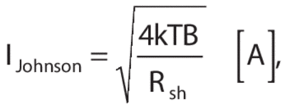
where k is Boltzman's Constant, T is the temperature in Kelvin, B is the bandwidth of the detector/amplifier, and Rsh is the shunt resistance of the photodiode. It can also be seen from this equation that a photodiode with a high shunt resistance is desired to reduce the Johnson Noise.
Shot noise is the noise produced by the flow of current in the diode and is given by,
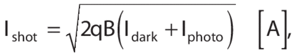
where q is the charge of an electron, Idark is the dark current, and Iphoto is the photocurrent. When a photodiode is used in the photovoltaic mode the voltage across the diode is kept at zero volts. Consequently, this almost eliminates the dark current altogether. Thus, the shot noise contributed by the dark current is also eliminated. To put these effects in perspective, if a detector were biased as in the photoconductive mode, the dark current would be about three decades larger than the noise equivalent current of an unbiased detector.
The photocurrent produced by the photodiode is measured directly by the power meter using an operational amplifier circuit known as a transimpedance amplifier. Typically, measurements can be made down to the sub-picoampere regime with good reproducibility, even at room temperatures. An exception to this rule is when the shunt resistance of the photodiode is small as with the Germanium photodiode (818-IR and 918D-IR). Because of its low shunt resistance (50 kΩ typical), tens of picoamperes can be resolved at best. Please see Photodiode Sensor Physics for additional information.
Thermopile Optical Sensor Basics
The basic laser high-power (>1 Watt) detector is essentially a thermopile. The more familiar application for thermopiles, in fact where the common name thermo electric cooler comes from, is when a voltage is applied to cool one side of the thermopile and whatever it is bonded to. However, thermopiles for laser power measurement are used in the opposite fashion. That is, a temperature difference is used to create a voltage. One side of the material is heated by the laser and the other side is a heat sink. The laser energy absorbed by that material is converted to heat. There is a temperature difference across the thermo electric device as the heat flows through it. This temperature difference causes the thermopile to generate a voltage. That voltage is proportional to the temperature difference, which is proportional to the laser power. The monitor measures this voltage to provide the laser power reading in Watts. Please see Thermopile Sensor Physics for additional information,
The Absorber
The optically absorbing material is one of the most important parts of the detector. That is because its properties define much of the performance of the detector, especially its resistance to pulse damage. This material absorbs most of the light energy from the laser and converts it to heat. A fraction is reflected that can vary from a few percent to 50 percent of the total optical power, depending on the material and intended application. How much is shown by the spectral absorptivity response curve for the material.
Volume Absorbers
For applications that require an extremely high concentration of power and energy in a small area and a small time period for a single wavelength, a volume absorber would be necessary. Unlike the broader band materials, which absorb the energy right on the surface, the energy is absorbed throughout the thickness of the material. Energy densities greater than 3 J/cm2 and peak power densities above 100,000 MW/cm2 can be handled this way depending on the wavelength.
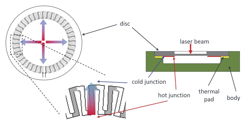
Disk Thermopiles
There are two kinds of thermopiles used in laser power measurement. One is the wafer type thermopile and the other is the disk. When a lot of average power is absorbed and has to flow through the small gap containing the thermocouples, the temperature becomes hot enough to damage the thermocouple junctions. That is when the disk thermopile shows its value. The disk is made of two sets of junctions laid out radially. One set of junctions is arrayed under the aperture while the alternate set is near the edge of the disk, which is attached to a massive heat sink. The laser power heats the absorber in the center and creates a temperature difference between the center and the edge. The thermocouples generate a voltage corresponding to this difference, just like in the wafer thermopile. The primary difference is that the heat flows radially through the disk, which can handle more average power, especially with blown air or water-cooling. The disk thermopile also has a much faster natural response time
Pyroelectric Detector Basics
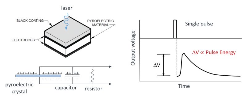
Pyroelectric detectors are designed to measure the energy of short optical pulses that have a maximum width of 5 to 400 µs, depending on the detector design. These detectors are made of a ferroelectric crystal that has a permanent dipole moment. When subjected to an optical pulse, the crystal is heated and causes the dipole moment to change. The changing of this dipole moment causes a current to flow, which is converted to a voltage in the detector head that can be measured by the optical power meter or oscilloscope.
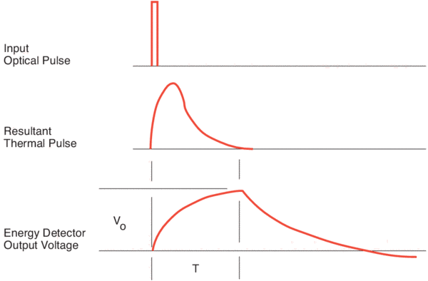
As shown in Figure 3, the resultant thermal pulse is broadened relative to the short optical pulse. During this thermal pulse, the current flows through the ferroelectric crystal, creating a voltage that increases in amplitude. The optical power meter has circuitry that measures the difference in voltage between when the output voltage just starts to increase and when the output voltage reaches its peak amplitude. This voltage difference is then numerically multiplied by the detector responsivity, which is in units of Joule/Volt, resulting in the energy of the pulse in units of Joules. Please see Pyroelectric Sensor Physics for additional information.
When using pyroelectrics, care must be taken not to exceed the maximum pulse width or the maximum repetition rate. If either of these specifications is exceeded, your measurement accuracy will degrade due to the electrical bandwidth limitation of the detector.
Photodiode Spectral Calibration
The detector calibrations are done using a double monochromator in order to minimize stray optical noise, especially in the ultraviolet. Three gratings and two light sources are used by the monochromator to maximize the signal to noise performance over the 200 to 1800 nm wavelength ranges. A deuterium lamp is used in the ultraviolet range up to 310 nm and a tungsten lamp is used thereafter in the visible and near infrared.
Newport uses two standard detectors that are sent to NIST with an exception of 818-IS and 918D-IS series detectors, which are sent to NRC (National Research Council Canada) for calibration on an annual basis. One of the standard detectors is used for the wavelengths between 200 to 1100 nm and the other for 780 to1800 nm. The absolute responsivity accuracy of NIST's standard detectors is based on a cryogenic radiometer which has a relative expanded uncertainty (k=2) to absolute SI units of 0.2%.
Prior to calibrating a manufacturing lot of detectors, the optical flux from the monochromator is measured in 10 nm steps using the NIST traceable standard detector throughout the wavelength range in which the detector-under-test (DUT) is to be calibrated. Since we know from NIST the responsivity of the standard detector, we calculate the optical flux of the monochromator using the following relationship:
Fluxmono ([W] = imeasured [A] / ResponsivityStd Det ([A/W]),
where imeasured is the measured current of the standard detector.
Knowing the flux coming from the monochromator, we measure the photocurrent of the DUT in 10 nm steps and divide this current by the monochromator flux to get the spectral responsivity of the detector in units of A/W.
Because the responsivity of a photodiode is temperature sensitive, especially near the ends of its usable wavelength range, we maintain the temperature of the standard detector and DUTs at the temperature where NIST calibrated the standard detector. This temperature control is critical for an accurate calibration. For example, silicon's temperature dependency induces a responsivity change of approximately 10% at 1100 nm with a 5°C change near room temperature.
Optical Power Meter Basics
Although most people want to make measurement in units of dBm or Watts, an optical power meter is only capable of measuring either the current or the voltage generated by a photodetector.
When interfacing with a photodiode, the quantity that must be measured is current. There are numerous techniques in measuring this current, but only one will yield the detectivity, signal-to-noise, and accuracy that is expected from a semiconductor photodiode. A circuit known as a transimpedance amplifier is the circuit of choice when using a photodiode (Figure 5).
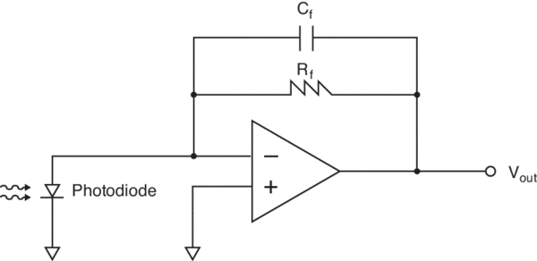
The advantage that the transimpedance amplifier has over almost any other amplifier configuration is that it does not bias the photodiode with a voltage as the current starts to flow from the photodiode. Typically, one lead of the photodiode is tied to the ground and the other lead is kept at virtual ground by means of the minus input of the transimpedance amplifier. The resultant bias across the photodiode is then kept at virtually zero volts, a condition that helps minimize dark current and noise, and helps increase linearity and detectivity.
Effectively the transimpedance amplifier causes the photocurrent to flow through the feedback resistor, which creates a voltage, V = iR, at the output of the amplifier. Since the meter knows the value of the precision feedback resistor, the current can be calculated with very good accuracy.
When interfacing with a thermopile or pyroelectric detector, voltage is the quantity that the optical meter must measure. There is, however, a considerable difference in how the measurement must be made between the two types of detectors. The optical meter's circuitry must be designed and configured to accommodate the two different types of voltage sources.
Thermopile detectors produce very slow bandwidth voltages (≈1 Hz) that can be measured in the sub-millivolt levels. One of the main concerns when trying to resolve such low voltages is to compensate for, or eliminate, thermoelectric voltages caused by dissimilar metals, which are generated in the connections and printed circuit board. It is somewhat ironic that the desirable physical effect that generates the voltage in a thermopile detector is similar to the undesirable effects that are present in the connections and printed circuit board. Precautions must be taken when choosing the electrical components to help minimize the unwanted thermoelectric voltages. Additionally, to accurately resolve small voltages, the optical meter must be able to zero any offset voltage due to temperature drift of the components and the thermopile.
Pyroelectric detectors, in contrast, produce relatively fast rise-time signals in the microsecond regime (see the figure in the Pyroelectric Basics Section). The circuitry in the optical meter must sample-and-hold both the baseline voltage and the peak amplitude of the pulse. These two voltages are then put into a differential amplifier; and it is this voltage difference that determines the amount of energy in the optical pulse by way of the responsivity of the detector. Precautions must be taken to avoid accidental triggering of the sample-and-hold circuit since these circuits are sensitive to noise. Because the faster pyroelectric detectors have narrow upper peaks, it is crucial that the bandwidth of the circuit is fast enough to capture the level of the upper peak without degradation of amplitude accuracy.
Integrating Spheres
Newport's general-purpose integrating spheres can be used to make a variety of measurements. Optional sphere accessories are also available to enhance their utility.
Measuring Beam Power
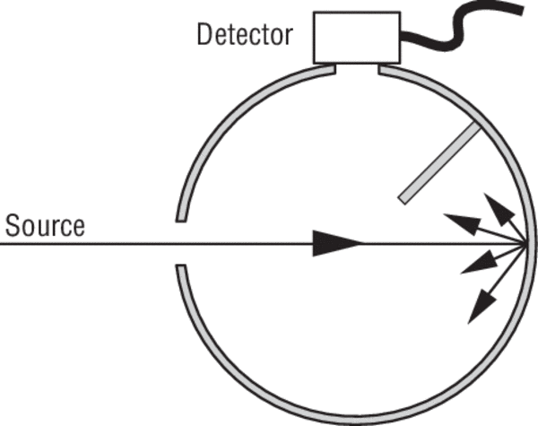
Measuring total collimated or uncollimated beam power (Figure 6), independent of polarization or beam alignment, is straightforward. The beam is admitted into the sphere and a detector, baffled from directly reflected radiation, that measures the spatially integrated beam power. Integrating spheres are ideal for measuring the output power of divergent beams from laser diodes, lensed LEDs and lensed lamps.
Measuring Transmittance
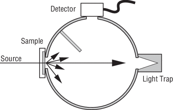
Transmittance (Figure 7) can be measured by using the integrating sphere to collect transmitted radiation from a sample held in one of the ports. The sample is irradiated, and then compared with a direct source measurement made outside the sphere. A baffle is used to shield the detector from non-integrated transmission, and a light trap can be used to remove the unscattered component. Measurements of total integrated scatter, fluorescence, bulk scatter and forward and back scatter can also be made.
Measuring Reflectance
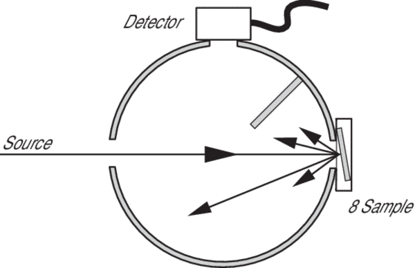
To measure reflectance, a sample is held in one of the ports and irradiated by an incident beam. Total reflected radiation is spatially integrated by the sphere and measured by a baffled detector. Using the normal-incidence sample holder, which reflects the specular beam back out of the input port, can eliminate the specular component of the reflective radiation. An 8°-incidence sample holder allows measurement of the "specular plus diffuse" reflectance (Figure 8). The reflectance of a sample relative to a known standard can be calculated by measuring both and taking their ratio. The sample and standard should have a similar reflectance to avoid errors caused by sample reflectivity. A dual-beam system can be used to eliminate this potential source of measurement error.
Measuring Fiber Optic Power Output
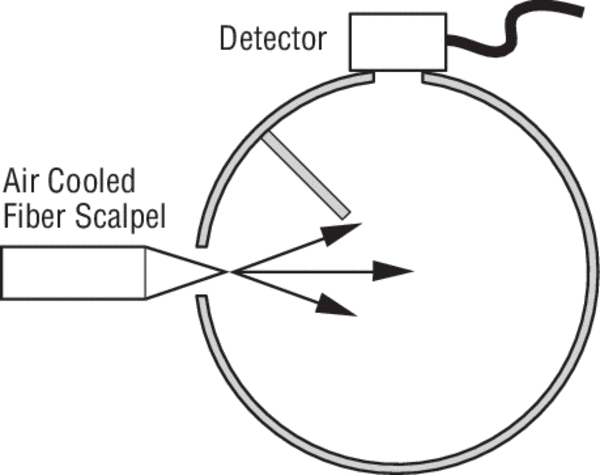
An integrating sphere is also ideal for measuring the output of optical fibers. In particular, this approach avoids the sensitivity of thermopiles to air currents and provides reliable NIST-traceable calibration of high-power, air-cooled fiber scalpels for surgical or ophthalmic applications (Figure 9).
Measuring Laser Diode Power
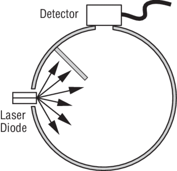
An integrating sphere and calibrated detector setup is suitable for accurate, absolute value light power measurement of laser diodes. Your measurements will be insensitive to problems associated with overfilling, or saturation, of the active area of the detector. A baffle, positioned between the input port and the detector port prevents the detector from directly viewing the emitting aperture of the laser or the direct area of illumination. In an integrating sphere, the detected flux is always a small fraction of the incident flux. This attenuation, caused by light reflecting many times before reaching the detector, makes the integrating sphere an ideal tool for measurement of output light power of high-power lasers (Figure 10).
Related Topics
Light Measurement and Characterization