Defect inspection for sub-100 nm patterned wafers presents greater challenges than for non-patterned wafer inspection. DUV-based optical inspection for patterned wafer applications uses the same image comparison principle as older VIS and UV light inspection systems. However, DUV-based methods require a much greater degree of sophistication in the optics, motion control, and image analysis algorithm.
DUV inspection tools have become the industry standard for patterned wafer inspection down to 65 nm feature sizes; inspection rates of up to several wafers per hour make these systems suitable for production applications. DUV inspection tools have demonstrated high sensitivities for the detection of defects such as shallow trench isolation voids, contact etch defects, and photoresist micro bridging at sub-100 nm geometries. Using broadband DUV/UV/VIS illumination, modern bright field patterned wafer inspection systems currently achieve the required sensitivity for defect inspection of all layers on DRAM and flash devices down to 55 nm feature sizes.
While their well-understood characteristics coupled with relatively low cost and high throughput make the continued use of DUV optical inspection systems attractive, some manufacturers have reported that DUV inspection systems do not have the needed precision and sensitivity for geometries below 65 nm. One study claims that the limiting defect sensitivity for DUV dark-field optical pattern inspection systems is about 75 nm in memory technology (e.g. SRAM) and much larger on logic areas. DUV bright-field systems have somewhat better limiting sensitivities, ~50 nm in SRAM and, as with dark-field, larger in logic. Furthermore, the use of DUV lasers to illuminate very small and consequently fragile structures on patterned wafers has produced some unusual problems such as laser ablation of surface material. The solution to these problems may lie in the use of either broadband plasma illumination for optical inspection systems (existing DUV systems employ 266 nm wavelength and are moving to 193 nm illumination) or in the use of production-capable electron beam inspection tools. Recently-introduced inspection tools based on plasma-generated broadband illumination are available for use in production environments. Sub-10 nm resolution is claimed for these systems, because shorter wavelengths provide more accurate inspection at this smaller scale.
Electron beam (EB) imaging is also used for defect inspection, especially at smaller geometries where optical imaging is less effective. EB inspection can provide material contrast with a dynamic range of resolution much larger than optical inspection systems. However, EB applications are limited by the slow speed of measurement, making it useful primarily in R&D environments and in process development for the qualification of a new technology. New EB tools are available for defect inspection applications at 10 nm and lower nodes, and multi-EB tools are being developed with up to 100 columns, or channels of measurement.
Reticles are transmissive or reflective projection masks patterned with fine features, typically 4x-5x larger than the desired pattern scale on the wafer. They are used with optical illumination systems that image and de-magnify the patterned light to selectively develop photoresists as part of the wafer patterning process.
Arguably, reticle inspection is far more important than either non-patterned or patterned wafer inspection. This is due to the fact that, while a single defect on a bare or patterned wafer has the potential to "kill" one device, a single, undetected defect on a reticle can destroy thousands of devices since the defect is replicated on every wafer processed using that reticle. With EUV this problem is further complicated by the finer resolution of the pattern, the presence of a thin protective membrane, and the reflective design of the reticle.
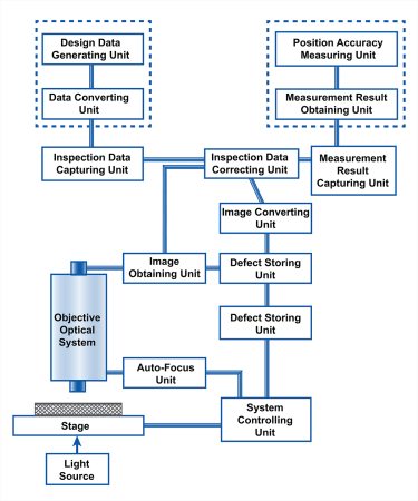
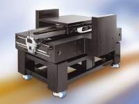
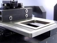
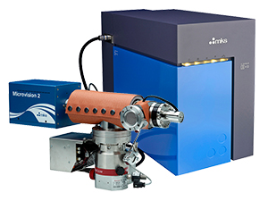
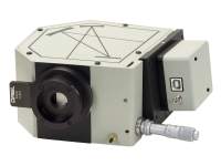
Reticle inspection systems work on the same principles and have similar physical requirements as wafer inspection tools, with the exception that reticles are normally inspected using transmitted rather than reflected light. Transmitted light is used to locate UV-opaque stains and other transmission defects. Reticle inspection tools employ high resolution imaging optics and either VIS or UV illumination, depending on defect tolerances and/or feature sizes, to find defects on a reticle blank or a patterned reticle. Inspections are routinely performed during the reticle manufacturing process and throughout the reticle usage. Reticle inspection tools employ sophisticated image analysis software and motion control systems similar to those used in wafer inspection tools. The use of conventional optics in reticle inspection systems has been extended down to 90 nm feature sizes by using UV illumination. Reticle inspection at smaller feature sizes is possible using EB since lower throughputs can be tolerated in comparison to patterned wafer inspection. As with wafer inspection, the reticle inspection tools used in sub-100 nm applications (both blank and patterned reticle inspection) employ DUV illumination, typically using a single wavelength at 266 nm or 193 nm. Figure 5 shows a block diagram of a reticle inspection platform. Note that, in addition to the objective optical system, motorized stage, and light source, the platform employs various controllers and data analysis modules. Reticle inspection systems can be configured to employ either transmitted light through the reticle or reflected light from the reticle surface in the inspection process. As with other inspection systems, this reticle inspection tool requires highly accurate and precise motion control for the optical components and the air bearing reticle stage.
 Over 8,000 products in-stock! & FREE 2-Day shipping on all web orders!* Learn More FREE T-Shirt with orders $250+ Details
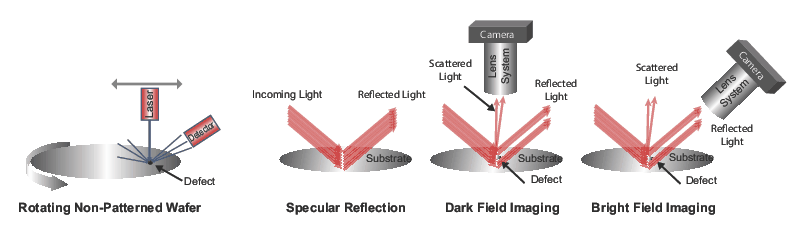


 Ultra-High Velocity