Patterned Wafer Inspection
The progression to ever smaller wafer feature sizes produces lower and lower tolerance to defects in both starting materials and finished devices. Not only are we approaching near zero tolerances to known defect types (particles, crystal defects, etc.), but manufacturers continue to discover device sensitivities to entirely new types of defects as manufacturing progresses into the deep nano-scale. In addition, the available metrologies for defect detection are being required to sense and quantify defects at very near the noise level of their operating principles and new approaches to defect detection are continually being developed.
Differential Image Detection
The optical inspection of patterned wafers can employ bright-field illumination, dark-field illumination, or a combination of both for defect detection. Patterned wafer inspection systems compare the image of a test die on the wafer with that of an adjacent die (or of a "golden" die known to be defect free). Image processing software subtracts one image from the other. Any random defect in one of the dies will not zero out in the subtraction process, showing up clearly in the subtracted image (Figure 1). The positions of the defects allow a defect map to be generated over the wafer, similar to the maps generated for non-patterned wafers. As with the inspection of non-patterned wafers, patterned wafer inspection requires precise and repeatable motion control of both the wafer stage and the optical components of the inspection system since they are moved simultaneously.

DUV Wafer Inspection for Sub-100 nm Features
Defect inspection for sub-100 nm patterned wafers presents greater challenges than for non-patterned wafer inspection. DUV-based optical inspection for patterned wafer applications uses the same image comparison principle as older VIS and UV light inspection systems. However, DUV-based methods require a much greater degree of sophistication in the optics, motion control, and image analysis algorithm.
DUV inspection tools have become the industry standard for patterned wafer inspection down to 65 nm feature sizes; inspection rates of up to several wafers per hour make these systems suitable for production applications. DUV inspection tools have demonstrated high sensitivities for the detection of defects such as shallow trench isolation voids, contact etch defects, and photoresist micro bridging at sub-100 nm geometries. Using broadband DUV/UV/VIS illumination, modern bright field patterned wafer inspection systems currently achieve the required sensitivity for defect inspection of all layers on DRAM and flash devices down to 55 nm feature sizes.
While their well-understood characteristics coupled with relatively low cost and high throughput make the continued use of DUV optical inspection systems attractive, some manufacturers have reported that DUV inspection systems do not have the needed precision and sensitivity for geometries below 65 nm. One study claims that the limiting defect sensitivity for DUV dark-field optical pattern inspection systems is about 75 nm in memory technology (e.g. SRAM) and much larger on logic areas. DUV bright-field systems have somewhat better limiting sensitivities, ~50 nm in SRAM and, as with dark-field, larger in logic. Furthermore, the use of DUV lasers to illuminate very small and consequently fragile structures on patterned wafers has produced some unusual problems such as laser ablation of surface material. The solution to these problems may lie in the use of either broadband plasma illumination for optical inspection systems (existing DUV systems employ 266 nm wavelength and are moving to 193 nm illumination) or in the use of production-capable electron beam inspection tools. Recently-introduced inspection tools based on plasma-generated broadband illumination are available for use in production environments. Sub-10 nm resolution is claimed for these systems, because shorter wavelengths provide more accurate inspection at this smaller scale.
E-beam Wafer Inspection
Electron beam (EB) imaging is also used for defect inspection, especially at smaller geometries where optical imaging is less effective. EB inspection can provide material contrast with a dynamic range of resolution much larger than optical inspection systems. However, EB applications are limited by the slow speed of measurement, making it useful primarily in R&D environments and in process development for the qualification of a new technology. New EB tools are available for defect inspection applications at 10 nm and lower nodes, and multi-EB tools are being developed with up to 100 columns, or channels of measurement.
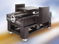
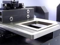
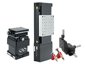
Motion Control for Wafer Inspection
We offer a variety of high performance air bearing stages suitable for use in wafer inspection tools and other motion control applications. The HybrYX™ XY Hybrid Air Bearing XY Stage is a relatively low cost, single plane air bearing stage that is well suited for semiconductor wafer inspection systems and many other scanning applications requiring ultra-low velocity ripple & dynamic following error. The HybrYX stage has a true single place XY architecture with available theta and Z-Tip-Tilt solutions. It features scanning velocities of up to 600 mm/sec and 0.6G acceleration and large (>1 meter) XY Travel range The HybrYX system has a demonstrated and reliable, long-life operation ideal for high duty cycle environments such as wafer inspection applications. The DynamYX® family of reticle positioning stages were specifically designed for semiconductor wafer processing and inspection applications. They offer the highest level of commercially available positioning performance. The extensive use of ceramic materials in these stages provides exceptionally rigid structural stability. They are designed with a low profile that aids in OEM applications.
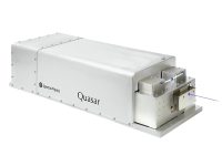
Custom Optical Solutions for Wafer Inspection
We offer optical sub-system design and manufacturing solutions for wafer inspection tool manufacturers. We have designed and manufactured optical sub-systems for lithography, wafer inspection, excimer and EUV light source, metrology and mask writing applications, among others.
Reticle Inspection Products


For additional insights into photonics topics like this, download our free MKS Instruments Handbook: Principles & Applications in Photonics Technologies
Request a Handbook