Optical Detection Systems
In a typical photo-research system, a detector measures the radiant intensity used to evoke photo-response in a sample or the radiant intensity produced by the sample in response to light or other simulation. The measurement is very frequently done after the beam has been separated into its component wavelengths. Light signals are converted into electrical signals, then typically amplified, processed by signal to noise improving electronics, and displayed. Computers are frequently utilized to present the measurements in a convenient form and in relation to other parameters such as wavelength or time. The combined detection and measurement system is called a radiometer. The term spectroradiometer is used when radiant intensity versus wavelength information is measured.
Detection systems are made possible by a few basic types of light-to-electrical signal conversion processes. Oriel detector systems can be roughly divided into:
- Thermal detectors
- Photon detectors
These are further divided by types of response generating processes. Wavelength and temporal response modifying phosphorescent accessories are used in some systems to adapt them to a particular UV measurement situation. Oriel detector systems typically consist of actual detector elements packaged with the appropriate bias, cooling, and signal processing electronics as needed for proper operation; many software options are available. A short introduction to the terms used when describing the elements themselves will facilitate later discussion of system selection criteria. Please excuse certain lack of scientific rigor in defining exactly under what circumstances the following descriptions apply. However, space limitations force us to omit a number of details.
Most detectors are described by certain figures of merit. You'll see these terms on the detector specifications pages. The figures of merit are usually function of wavelength and temperature and may also be affected by detector size, modulating frequency, bias voltage and the gain of any internal amplifier. We define them below.
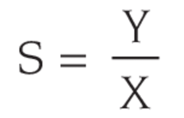
Responsivity (s)
Where:
Y = detector output
X = radiation input
Examples of Y include current or counts from a photomultiplier or voltage from a thermopile. Y usually has a value Y0 (dark signal) for X = 0. In this case
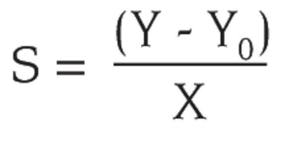
X can be any radiative input. The units of X are usually watts or lumens. In cases of uniform irradiance on the detector, X may be given as the product of the irradiance and detector area.
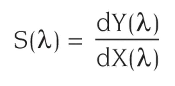
S is usually wavelength dependent. The variation with wavelength is described by the Spectral Responsivity S(λ)
Where:
dY(λ) = the fraction of output due to input dX(λ) at λ
Quantum Efficiency (η)
This is the ratio of the number of basic signal elements produced by the detector to the number of incident photons. The basic signal element is frequently a photoelectron.
Reponse Time (τ)
τ is the time it takes a detector's output to rise when suddenly subjected to constant irradiance. When the irradiance is turned off, the detector output falls to 1/e of the initial value in one time constant. The rise and fall time constants are frequently different, since different physical parameters may cause them.
Linearity Range
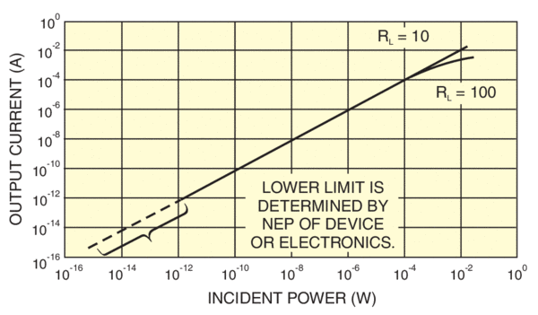
This is the range of input radiant flux over which the signal output is a linear function of the input. The range is often stated in terms of input watts or input irradiance. It usually extends from the noise equivalent power level to an upper limit which may be device or external circuit limited.
Noise Equivalent Power (NEP)
NEP is the radiant flux in watts necessary to give an output signal equal to the r.m.s. noise output from the detector. The flux may be either continuous or sinusoidally modulated.
The response is assumed to be linear down to the noise level. NEP values should be stated at a specified wavelength, modulation frequency, detector area, temperature and detector bandwidth. Detector bandwidth is usually normalized to 1 Hz and NEP is frequently quoted in watts Hz-1/2.
NEP is the most commonly used version of Noise Equivalent Detector Input (PN).
Detectivity (D)
D is the reciprocal of NEP. It is given by:
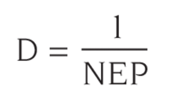
This gives a figure of merit which is larger for more sensitive detectors.
Normalized Detectivity (D*)
For most detectors DAD1/2 is constant; i.e., the detectivity varies inversely with the square root of the area of the detector. This is because the electrical noise power is usually proportional to the detector area AD, and current or voltage, which provide a measure of that noise, are proportional to the square root of power. Similarly, because most detector noise is white noise, and white noise power is proportional to Δf (where Δf is the electrical bandwidth), the noise signal is proportional to Δf1/2.
D* is defined to allow comparison of different types of detectors independent of the detector area and bandwidth.
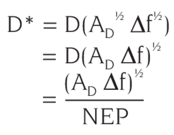
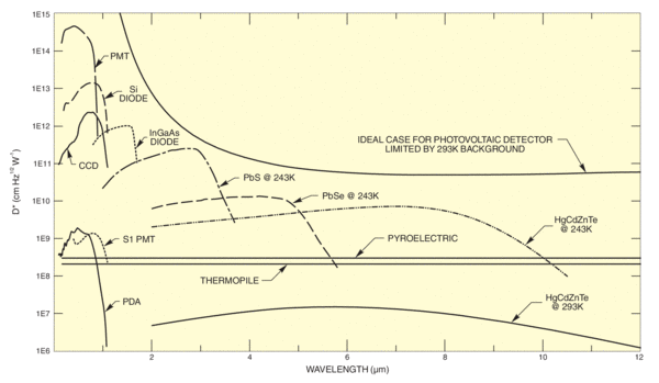
The units of D* are cm Hz1/2 W-1. Since D*, like NEP, is a function of wavelength and modulation frequency, it is common to see the normalized spectral responsivity D*(λ), or D*(λ,f,Δf). Figure 2 shows the D* of a number of our detectors.
Noise
So far we have not specified the nature of the noise which limits the detectivity. There are several types:
- Shot noise
- Generation-recombination noise
- Johnson noise
- Flicker or 1/f noise
- Readout noise for array detectors
Shot Noise is due to the discrete nature of radiation, which is composed of photons arriving randomly in time. Absorbed photons produce photoelectrons at random intervals, and this variation in current appears as noise. This noise can be generated by actual desired signal photons or, in case of very low signal and very low noise detectors, by background photon flux. When that occurs, the detector system is said to operate in a Background Limited in Performance (BLIP) mode.
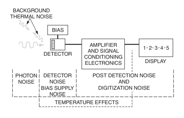
Generation-recombination Noise is seen in photo-conductors in which the absorbed photons produce both positive and negative charge carriers. Some of the free carriers may recombine before they are collected. Thermal excitation may generate additional carriers. Both the generation and recombination occur randomly, resulting in noise fluctuations in the output current.
Johnson Noise or thermal noise is caused by the random motion of carriers in a conductor. The result is fluctuations in the detector’s internal resistance, or in any resistance in series with the detector's terminals.
Flicker or 1/f Noise is not well understood. It occurs in detectors such as photoconductors which require a biasing current. Its magnitude is proportional to 1/fB where B is usually between 0.8 and 1.2.
Readout Noise is a characteristic of array detectors and is associated with the uncertainties introduced during the transfer of charges between storage registers.
In addition to the sources described above, detector signals can be subject to microphonic noise, caused by vibration or shock and by post detector electronic noise. Often the circuitry after the detector determine the lowest measurable signal, particularly for detectors which do not provide some internal amplification of the photocurrent. By contrast, the almost noise-free internal amplification of photomultipliers accounts for their superb performance.
Finally, detectors are subject to temperature noise caused by fluctuations in their temperature. This can be a problem for small thermal detectors with low thermal mass.
Calibration
There are a lot of measurement situations when the knowledge of the exact magnitude of an effect is not needed. A relative reading is all that is necessary. In that case we only have to make sure that the inputs are higher than the NEP level and lower than the damage level. Measurements become much simpler if the inputs are also within the linear range of the detection system response.
However, when absolute measurements are required to quantify the light flux, calibrated instruments are needed. Our Calibration Laboratory has acquired a number of National Institute of Standards and Technology (NIST) source and detector calibration standards, as well as additional standards traceable to international standards’ setting and disseminating bodies. We are also in the enviable position of being able to utilize our own broad range of products: UV and IR light sources, detectors, electronics, optics, positioning equipment, monochromators, spectrographs, and FT-IRs, to provide single point or spectrally resolved calibration for most of the detector products we ship. For some detectors we offer optional PROMS that store a wavelength-responsivity table. We use our calibration transfer standards, lamps and detectors, typically traceable to the national Institute of Standards and Technology (NIST) to ensure meaningful and reproducible calibrations.
Thermal Detectors
Thermal detectors work by converting the incident radiation into a temperature rise. The temperature change can be measured in several ways. Our detectors use either the voltage generated at the junction of dissimilar metals, or the pyroelectric effect. In either case, we have a “sensitive element” where we measure temperature change.
We blacken the sensitive element to enhance the absorption of the radiation. We choose the blackening material for its high and nearly uniform absorption, and hence detector responsivity, over a wide spectral range. This is a major advantage of thermal detectors.
The thickness of the black absorber is controlled to avoid adding excessive thermal mass to some detectors. High thermal mass slows the response time and typically increases NEP.
We offer two types of Thermal Detectors:
1. Thermopile Detectors for DC radiation.
2. Pyroelectric Detectors for pulsed, chopped or modulated radiation.
Thermopiles
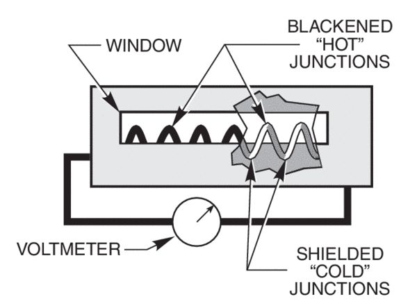
One way to increase the output voltage is to connect a number of the thermocouple junctions (typically 20 to 120) in series. All the “hot” junctions are placed close together to collect the radiation. This constitutes a thermopile. Thermopiles can be produced economically by thin film processes, yielding rugged units suitable for field use. These have time constants ranging down to below 50 ms, in small sizes with metal oxide blackening. Larger thermopiles, made with individual wire junctions backing up a highly absorbing black disk, have long time constants, more than a second in many cases. Please see Thermopile Sensor Physics for additional information.
Thermopiles exhibit no flicker, 1/f, noise, since no current bias is needed to operate them. Highly sensitive measurements can be made from DC to the few Hz frequency response limit of a particular device.
These devices are quite sensitive in the infrared, thanks to their broadband absorption. Therefore, care must be taken to stabilize their field of view, since all near room temperature objects, including people, emit significant IR. Measurements are best made by shuttering the radiation falling on the detector and observing the change in output voltage. It is not uncommon to see "negative" radiation if the source is cooler or less emissive than the shutter used to get “zero” reading.
Pyroelectric Detectors
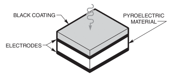
A pyroelectric material has electric polarization even in the absence of an applied voltage. The materials are usually crystalline. On heating, the material expands and produces a change in the polarization which builds up a charge on opposite surfaces. This causes a current to flow in the circuit which connects the surfaces.
Since it is the change in temperature which produces the current, pyroelectric detectors respond only to pulsed or modulated radiation. They respond to variations in radiation much more rapidly than thermocouples or thermopiles and are unaffected by steady background radiation. Small detectors with small thermal mass can have extremely rapid response. Adding a black coating to give uniform absorption over a wide spectral range increases the mass and lowers the frequency response. This is significant as typical pyroelectric elements may be only 25 µm thick, while the coating is 75-100 µm thick.
The response of a pyroelectric detector depends on two time constants. The thermal time constant determined largely by the thermal mass and the thermal connections from the element to its surroundings, and the electrical time constant which is the product of the shunt resistance and shunt capacitance of the detector/amplifier circuit.
Our pyroelectric detectors are designed for operation in two different modes:
1. As detectors of isolated or relatively infrequent (<4000 Hz) radiation pulses. The pulses may vary in width from picoseconds to milliseconds and in energy from nanojoules to joules.
2. As detectors of modulated or chopped radiation, where the detector produces an AC output signal.
The thermal and electrical time constants of pulse measuring detectors are chosen so each pulse is integrated. The peak of the output voltage is a measure of the charge produced by the detector and therefore of the pulse energy. The charge dissipates before the arrival of the next pulse. The relatively long integration time, or fall time, imposes limitations on the minimum interval between pulses or the repetition rate of pulses which can be individually measured.
The chopped mode or modulated radiation detectors are much different. They are frequently used in FT-IR and lock-in detection type applications. In FT-IR instruments, the pyroelectric detector follows the modulated signal and produces the interferogram which is then transformed into a spectrum information. In a lock-in setup, the measured radiation has a 50% duty cycle and the output signal is the average of a large number of chopping cycles. A lock-in detection system is used to remove most of the background radiation influence on readings. The natural 100-200 Hz level response frequency limit of these pyroelectric detectors is electronically extended to the 1 kHz level to facilitate fast chopping. This is sometimes needed to remove background noise in thermally fast changing environments. However, the chopping frequency should be below 200 Hz for best inherent noise performance. Please see Pyroelectric Sensor Physics for additional information.
Photon Detectors
Photon or Quantum detectors respond to the incoming photon flux in a quantized manner. They produce, under perfect conditions, a single response element for a single photon. Of course, perfect conditions are not usually found in nature, therefore you must account for insufficiencies of response.
The single response elements can take on various forms. They can be a photoelectron in a detector with photoemissive sensor, such as a photomultiplier tube; or an electron-hole pair separating in a junction photodiode, the basis of operation of silicon detectors; or an electron elevating from a valence to conduction band in photoconductors, as in a lead sulfide detector. The net result is either a change in current flow or voltage level which can then be processed by amplifiers and other electronics into a display or recording.
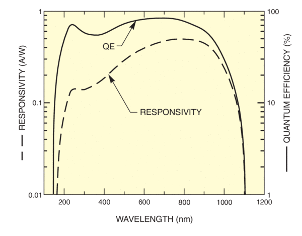
Before we discuss the different inefficiencies of conversion of photons to electrical signal, we should mention one significant difference between thermal and photon detectors. Thermal detectors respond to heat. This means that one watt delivered by 200 nm UV photons, produces the same response as one watt delivered by 10 µm infrared photons. Photon detectors produce at most one response element, prior to any amplification, per incoming photon. The energy carried by individual photons is inversely proportional to their wavelength. Therefore, for the same radiant power, the photon flux is much lower in the UV than in the IR. Accordingly, photon detector responsivity, in terms of V/W or A/W, is significantly lower in the ultraviolet part of the spectrum than in the infrared. When evaluating detector absolute performance it is important not only to look at the responsivity curves, vital as they may be to your actual application, but also at the quantum efficiency (QE) curves. The QE curve shows what percentage of the incoming photon flux is being converted into electrical signals, the efficiency of the detector. A relative responsivity curve for a 100% efficient photon detector is shown in Figure 6.
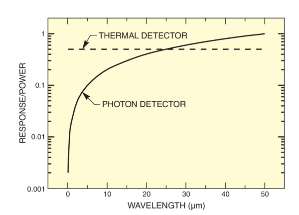
Figure 7 demonstrates a typical responsivity curve of a silicon detector and the corresponding quantum efficiency curve. We use it to discuss some of the inefficiencies in converting the incoming photon flux into an electrical signal. An ideal silicon detector has zero responsivity and quantum efficiency for photons with energies less than the band gap energy, or wavelength longer than approximately 1.1 µm. Just below the long wavelength limit the responsivity and QE should shoot up to approximately 0.9 A/W responsivity and 100% efficiency corresponding to each of the incident photons being converted into a single electron worth of charge. For all the shorter wavelength photons we could expect 100% quantum efficiency and the responsivity to behave in a fashion similar to the curve in Figure 7.
We see in Figure 7 some of the features we were expecting but the onset of the responsivity is not as sudden as expected; we never get to 100% quantum efficiency, and we lose efficiency again at short wavelengths.
Photoemissive and Semiconductor Junction Detectors
Common Characteristics
Photoemissive and semiconductor detectors have much in common.
1. The direct photo-electron interaction is very rapid so these detectors have the potential of following fast changing radiation levels.
2. Detectivity is in general higher than that of thermal detectors, but over a limited wavelength range.
3. All the detection mechanisms are wavelength dependent; i.e. there is a peak in responsivity with a fall off at both long and short wavelengths (Figure 8). The long wavelength (low photon energy) cut-off occurs because there is a certain minimum photo energy required to cause photo emission, to produce charge carriers, or to generate hole-electron pairs.
The short wavelength cut-off is a function of two effects:
1. The responsivity in terms of power drops off because there are fewer short wavelength photons per watt, see Figure 7.
2. At the extreme short wavelength end, the energetic photons may no longer be absorbed in the sensitive region. In the deep ultraviolet, absorption of the photons before they reach the sensitive region is also a problem. Detector windows, or surface coatings can also contribute to the spectral shape of the responsivity curve.
Between the upper and lower cut-offs, the quantum efficiency (events per photon) is approximately constant. It can be strongly affected by Fresnel reflection from the surface of the detector. For example, for the high index of refraction silicon diodes, surface reflection accounts for most of the departure from 100% quantum efficiency in the middle wavelength region.
The long wavelength cut-off in response is softened by the associated fall off of the absorption coefficient. A lower absorption coefficient means that more photons pass through the thin photosensitive layers. These photons do not contribute to the quantum efficiency. This causes gradual roll off of quantum efficiency near the band gap limit, the long wavelength cut-off.
Photomultiplier Tubes, PMTs
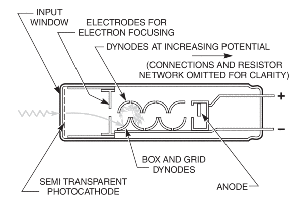
In a photoemissive detector, light interacts directly with the electrons in the detector material. An absorbed photon frees an electron and the surplus energy gets converted into kinetic energy of an electron. Electrons with enough kinetic energy escape from the surface. The electrons emitted in this way produce the cathode photocurrent in photomultiplier tubes. An applied voltage causes the electrons to flow toward the anode, creating a current that can be proportional to light intensity over 6 to 8 orders of magnitude. The electron multiplier part of a photomultiplier tube amplifies the photocurrent by secondary emission. This is a low noise process which produces currents that are orders of magnitude larger than the initial photocurrent. Photomultipliers are more sensitive than any other detector in the near UV and visible regions.
Figure 8 shows a schematic depiction of an end-on tube. Our side-on tubes have similar components arranged in a much tighter geometry which makes packaging easier and removes some of the environmental sensitivities of these superb detectors. The end-on tubes have larger and more uniform photosensitive areas; side on tubes have faster risetimes and reach higher responsivities since most of them use opaque photocathodes, thus avoiding the optical losses associated with the semitransparent photocathodes of the end-on tubes. Since nothing in life is simple, our fastest side-on tubes use a semitransparent photocathode because it allows even tighter packaging of the electron-multiplying dynode chain.
The stability of the electron multiplying process depends on the electrons following fairly exact trajectories. Magnetic fields can affect the directions of such electron flow in a significant manner, since the tubes are physically large. This is particularly noticeable in the end-on PMTs. You will find magnetic shielding, such as offered in our housings, to greatly improve your measurement reproducibility.
These DC biased detectors, with 1 kV level bias voltages and voltage divider network currents of 100s of µA, are characterized by flicker, 1/f noise. However, their excellent responsivity still allows them to function very well as DC detectors. Narrow bandwidth AC detection such as with our Merlin™ Digital Lock-in Amplifier, makes their already low NEP levels drop even further, fW Hz-1/2 levels are typical. Photon counting mode of operation allows you to reach NEP levels of 10-19 W Hz-1/2.
Junction Photodiodes
There are several ways of classifying semiconductor detectors. All are photoconductive, but here we use the photoconductive detectors' name for devices which rely on photoconductivity in the bulk and do not necessarily have junctions.
Junction detectors (or photodiodes) have a p-n junction formed in them. Many junction detectors can be used in the photovoltaic mode without a bias, or in the photoconductive mode when a reverse bias is applied. They can also provide photocurrent amplification through an avalanche ionization process when back biased at near breakdown voltage in properly designed structures.
In the photovoltaic mode, the electron-hole pairs (produced by photon absorption) migrate to opposite sides of the junction thus producing a voltage (and also a current, if the device is connected in a circuit).
In the photoconductive mode, a reverse bias is applied across the junction. Light produces electron-hole pairs which greatly increase the conductance. The current produced by the bias and free carriers is proportional to the light intensity over a wide range.
Silicon Photodiodes
Silicon photodiodes are the most common detectors of light used in instrumentation. The spectral response covers the UV, the visible and the near infrared. The linearity and dynamic range are excellent; getting a signal is simple.
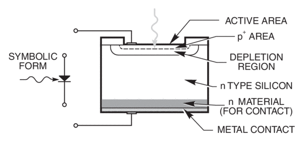
Figure 9 shows the typical structure of a silicon photodiode. Photons pass through the thin top layer to generate electrons and holes near the junction. The junction is a region depleted of current carriers, both electrons and holes, by the gradients of the potentials associated with the energy bands. It is formed between the p and n type silicon. The junction drives holes into the p material and the electrons into the n material. This results in a voltage difference between the two regions, and if they are connected by external circuitry, a current. Please see Photodiode Sensor Physics for additional information.
Unbiased Operation - Photovoltaic Mode
Because the 1/f noise increases with bias, this mode has the better NEP at low frequencies. In fact the signal to noise ratio is better than that for biased operation at frequencies below 100 kHz and much better below 1 kHz.
Biased Operation - Photoconductive Mode
Operation with reverse bias reduces junction capacitance and thus increases the speed of response of the diode. It is the preferred mode of operation for pulsed detectors.
Linear Range
Silicon diodes require a low impedance load resistor to provide a linear output in a photovoltaic mode. This makes the maximum output voltage too low to achieve wide dynamic range when using an oscilloscope as a monitor. A transimpedance amplifier solves the major linearity restrictions, by providing near "zero" load impedance, and produces higher output voltages. It also limits the high frequency response of the system.
Wide range linear performance is much easier to achieve in the back biased mode of operation. Linear output persists almost all the way to bias voltage allowing easy display on an oscilloscope. We provide 6 V back bias from long life lithium batteries for our biased detectors.
InSb
These liquid Nitrogen cooled detectors, used with our FT-IR instruments, offer ultimate performance in the 2 to 5 µm range.
Ge, InGaAs, Extended InGaAs Photodiodes
Just about everything we said about silicon detectors can also be said about the these diodes. They find most applications in the NIR, 0.8 to 2.5 µm. Their noise performance does not match that of Si and therefore we offer TE cooled versions of them, besides the room temperature ones.
HgCdZnTe Photodiodes
Things get even more confusing as far as junction photoconductors vs bulk photoconductors with these small band gap IR photodetectors. However, at least one room temperature implementation of these detectors does function in a photovoltaic mode and thus deserves to be listed in this section. Their current biased versions fit better with the PbS and PbSe photoconductors than with back biased junction diodes.
We offer these detectors for the 2 to 12 µm wavelength range. Optical immersion is offered with most of them to take better advantage of the detector active area.
Multichannel Detectors
The detectors we've been describing until now are single, discrete devices. Now we talk about multichannel detectors - photodiode arrays and charge coupled devices. The major differences between them lie in sizes of sensitive elements or pixels, the linear versus two dimensional value of the arrays, and the signal handling and readout methods. Our LineSpec™ detector utilizes silicon as a detector and are therefore sensitive in the 200 to 1100 nm spectral range.
The most useful arrays, and the only kind in our catalog, are of a self scanning type. This means that individual detector elements, and their associated circuitry, integrate the incident photon flux for some time and then are read out in a serial fashion. This is significantly different from the real time operation of single element detector systems. This self scanning mode of operation limits the nine or ten orders of magnitude dynamic range of individual photodiodes to a more practical three to five orders of magnitude, device dependent. High density packing of the small photosensitive pixels, to minimize non-photoresponsive areas and provide high resolution, limits the capacity of the charge storing structures. The major benefit of this charge storage capability is that usually only a single data channel is needed to read the information from all the spectral or imaging channels.
All arrays share the major advantage of multichannel or multiplexing capability. They make possible an almost instantaneous acquisition of one or more full spectroradiometric data sets when coupled to a standard or imaging spectrograph. The traditional technique would have involved mechanical scanning of one or more monochromators to sequentially bring various wavelengths of light to the single detector location.
LineSpec™ Charge Coupled Devices (CCD)
This inexpensive linear CCD detectors, with 2048 pixels, allows high speed, low cost data collection, for intermediate illumination level applications.
Photoconductive Detectors
In photoconductive detectors, absorbed incident photons produce free charge carriers. These change the electrical conductivity of the detector. An applied voltage, or bias, causes a current to flow which is proportional to the photon irradiance (it helps if the dark resistance is very high). Lead sulfide and lead selenide are examples of this type of detector. Figure 10 shows this concept.
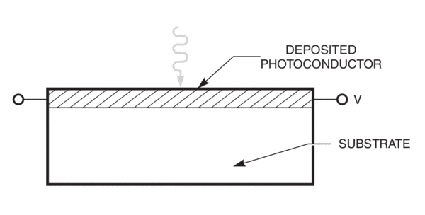
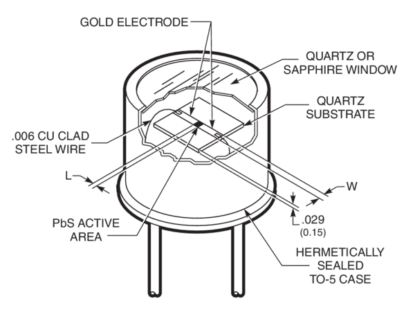
PbS and PbSe detectors are fabricated by chemically depositing polycrystalline film on a quartz substrate. Gold electrodes are plated to the edges of the film to provide electrical contact and the whole assembly is sealed inside a package with an appropriate window, quartz or sapphire. See Figure 11. The cooled lead salt detectors also include the TE cooling stages and a thermistor sensor inside of the housing. This minimizes the cooling requirements, since the housing minimizes heat transfer from the environment to the detector element. The heat being generated by the TE coolers also protects the window from condensation.
Liquid Nitrogen cooled MCT detectors, used in our MIR 8000™ FT-IR instruments, offer ultimate detectivity in the 2 to 17 µm range. The TE cooled HgCdZnTe family offers somewhat lower performance, but removes the need for liquid nitrogen refilling.
The epitaxially grown HgCdZnTe family of detectors is characterized by low impedance, but when properly biased and interfaced also provides linear performance. This versatile room and near room temperature operation family of detectors does not exactly fit either the junction or bulk photoconductor description. However, it is similar to one or the other in its different modes of operation. In the photoconductive mode of operation it is characterized by significantly faster risetimes than the lead salt detectors, especially at longer wavelengths.
Bias requirements, and the associated heating, as well as noise generation is smaller in smaller detectors. One way to make a small detector look optically like a big detector is through the use of optical immersion, Figure 12.
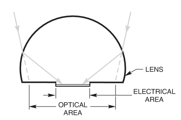
This approach makes the detector surface look n⊃2; times larger, where n is the index of refraction of the lens, for the hyperspherical lens shape. The monolithic construction of these detectors, (the epitaxial layer is grown directly on the lens substrate) makes this approach highly effective for HgCdZnTe detectors.
