Technical Note:
Introduction to FTIR Spectroscopy
A Fourier Transform InfraRed (FT-IR) Spectrometer is an instrument which acquires broadband Near InfraRed (NIR) to Far InfraRed (FIR) spectra. Unlike a dispersive instrument, i.e. a grating monochromator or spectrograph, FTIR spectrometers collect all wavelengths simultaneously. This feature is called the Multiplex or Felgett Advantage.
FT-IR Spectrometers are often simply referred to as FTIRs. But for the purists, an FT-IR is a method of obtaining infrared spectra by first collecting an interferogram of a sample signal using an interferometer, and then performing a Fourier Transform (FT) on the interferogram to obtain the spectrum. An FT-IR spectrometer collects and digitizes the interferogram, performs the FT function, and displays the spectrum.
Why an FT-IR Spectrometer?
Choose an FT-IR over a dispersive instrument if:
- The spectral region is in the infrared
- High spectral resolution is required
- The application involves weak signals
- The spectra needs to be acquired quickly with high S/N ratio
- High spectral accuracy is required
Due to their inherent design, FT-IRs excel in all of these categories. How much of this potential advantage is realized in an application depends strongly on the instrument’s design and the particulars of the measurement.
How Does an FT-IR Spectrometer Work?
The Michelson Interferometer
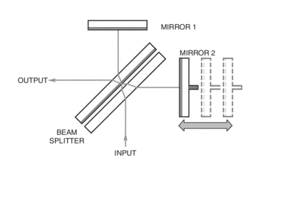
An FTIR is typically based on The Michelson Interferometer Experimental Setup; an example is shown in Figure 1. The interferometer consists of a beam splitter, a fixed mirror, and a mirror that translates back and forth, very precisely. The beam splitter is made of a special material that transmits half of the radiation striking it and reflects the other half. Radiation from the source strikes the beam splitter and separates into two beams. One beam is transmitted through the beam splitter to the fixed mirror and the second is reflected off the beam splitter to the moving mirror. The fixed and moving mirrors reflect the radiation back to the beamsplitter. Again, half of this reflected radiation is transmitted and half is reflected at the beam splitter, resulting in one beam passing to the detector and the second back to the source.
What are OPD and ZPD?
Optical Path Difference (OPD) is the difference between the two beams travelling through the two arms of an interferometer. OPD is equal to the product of the physical distance travelled by the moving mirror (multiplied by 2, 4, or other multiplier, which is a function of the number of reflecting elements used) and n, the index of refraction of the medium filling the interferometer arms (air, Nitrogen for purged systems, etc.). The raw FT-IR data consists of pairs of values (signal, OPD, etc).
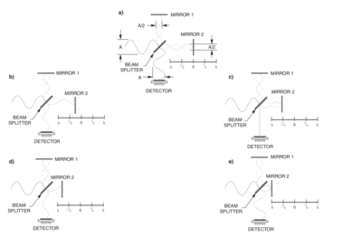
FT-IR has a natural reference point when the moving and fixed mirrors are at the same distance from the beam splitter. This condition is called the zero path difference or ZPD. The moving mirror displacement, Δ, is measured from the ZPD. In Figure 2 the beam reflected from the moving mirror travels 2Δ further than the beam reflected from the fixed mirror. The relationship between the optical path difference and mirror displacement, Δ, is:
OPD = 2Δn
The Interferogram
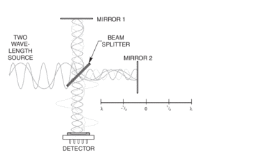
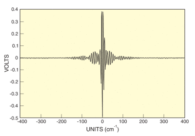
Interferogram is the name of the signal format acquired by an FT-IR spectrometer. It is usually significantly more complex than a single sinusoid, which would be expected if only a single wavelength of light was present. Figure 3 shows the beam path of a two wavelength source; Figure 4 is the interferogram of a broadband light source. The centerburst, the big spike in the center of Figure 4 is a telltale signature of a broadband source. Its origin lies in the fact that all wavelengths are in-phase at the ZPD. Therefore, their contributions are all at maximum and a very strong signal is produced by the system’s detector.
As the optical path difference, OPD, is increased, different wavelengths produce peak readings at different positions, and for a broadband signal, they never again reach their peaks at the same time. Thus, as we move away from the centerburst, the interferogram becomes a complex oscillatory signal with decreasing amplitude.
The X-axis of the interferogram represents the optical path difference. Each individual spectral component contributes a single sinusoid with a frequency inversely proportional to its wavelength to this signal. This leads us to the definition of the unit of spectral measurement: the wavenumber (cm-1), denoted as n. A wavenumber represents the number of full waves of a particular wavelength per cm of length (typically in vacuum, where the index of refraction n=1). The advantage of defining the spectrum in wavenumbers is that they are directly related to energy levels. A spectral feature at 4,000 cm-1 spectral location represents a transition between two molecular levels separated by twice the energy of a transition with spectral signature at 2,000 cm-1.
Table 1 lists a sampling of corresponding wavelength, wavenumber, frequency and energy values.
Table 1 Corresponding Values for Different Units of Measure
| ν (cm-1) |
λ (µm) |
f (1012 Hz) |
E (eV) |
|---|---|---|---|
| 200 | 50 | 5.996 | 0.02479 |
| 500 | 20 | 14.99 | 0.06199 |
| 1000 | 10 | 29.98 | 0.12398 |
| 2000 | 5 | 59.96 | 0.24797 |
| 5000 | 2 | 149.9 | 0.61922 |
| 10,000 | 1 | 299.8 | 1.23984 |
The Fourier Transform Algorithm
Once an interferogram is collected, it needs to be translated into a spectrum (emission, absorption, transmission, etc.). The process of conversion is through the Fast Fourier Transform algorithm. The discovery of this method by J.W. Cooley and J.W. Tukey in 1965, followed by an explosive growth of computational power at affordable prices, has been the driving force behind the market penetration of FT-IR instruments.
A number of steps are involved in calculating the spectrum. Instrumental imperfections and basic scan limitations need to be accommodated by performing phase correction and apodization steps. These electronic and optical imperfections can cause erroneous readings due to different time or phase delays of various spectral components. Apodization is used to correct for spectral leakage, artificial creation of spectral features due to the truncation of the scan at its limits (a Fourier transform of sudden transition will have a very broad spectral content).
FT-IRs are capable of high resolution because the resolution limit is simply an inverse of the achievable optical path difference, OPD. Therefore, a 2 cm OPD capable instrument, such as our FTIR scanner model 80351, can reach 0.5 cm-1 resolution. Table 2 shows the relationship between resolution expressed in wavenumbers and in nanometers, as is customary in dispersive spectroscopy.
Table 2 Resolution Values in Wavenumbers and Nanometers
| Wavelength (µm) |
Resolution (cm-1) |
Resolution (nm) |
|---|---|---|
| 0.2 | 1 | 0.004 |
| 0.5 | 1 | 0.025 |
| 1 | 1 | 0.1 |
| 2 | 1 | 0.4 |
| 5 | 1 | 1.0 |
| 10 | 1 | 10 |
| 20 | 1 | 40 |
Advantages of FT-IR Instruments Over Dispersive Instruments
Following, we talk about three significant advantages that FT-IR instruments hold over dispersive spectrometers, but first we compare the two instruments.
Table 3 FT-IR and Dispersive Spectrometer Comparison
| MIR 8035™ FT-IR Scanner | Cornerstone™ 260 1/4 m Grating Monochromator | |
|---|---|---|
| Wavelength Range | 700 nm - 25 µm | 180 nm - 24 µm |
| Max. Resolution | 0.024 nm @ 700 nm | 0.25 nm with 10 um slit and 1200 line/mm grating @ blaze wavelength |
| Etendue @ 1 µm, 0.15 nm resolution | 0.38 @ 1 µm, 0.15 nm resolution | 0.002 |
Multiplex (Fellgett) Advantage
In a dispersive spectrometer, wavenumbers are observed sequentially, as the grating is scanned. In an FT-IR spectrometer, all the wavenumbers of light are observed at once. When spectra are collected under identical conditions (spectra collected in the same measurement time, at the same resolution, and with the same source, detector, optical throughput, and optical efficiency) on dispersive and FT-IR spectrometers, the signal-to-noise ratio of the FT-IR spectrum will be greater than that of the dispersive IR spectrum by a factor of √M, where √M is the number of resolution elements. This means that a 2 cm-1 resolution, 800 - 8000 cm-1 spectrum measured in 30 minutes on a dispersive spectrometer would be collected at equal S/N on an FT-IR spectrometer in 1 second, provided all other parameters are equal.
The multiplex advantage is also shared by Array Detectors (PDAs and CCDs) attached to spectrographs. However, the optimum spectral ranges for these kinds of systems tend to be much shorter than FT-IRs and therefore the two techniques are mostly complementary to each other.
The Throughput Advantage
FTIR instruments do not require slits (in the traditional sense) to achieve resolution. Therefore, much higher throughput with an FTIR can be achieved than with a dispersive instrument. This is called the Jacquinot Advantage. In reality there are some slit-like limits in the system, due to the fact that one needs to achieve a minimum level of collimation of the beams in the two arms of the interferometer for any particular level of resolution. This translates into a maximum useable detector diameter and, through the laws of imaging optics, it defines a useful input aperture.
High Resolution
Spectral resolution is a measure of how well a spectrometer can distinguish closely spaced spectral features. In a 2 cm-1 resolution spectrum, spectral features only 2 cm-1 apart can be distinguished. In FT-IR, the maximum achievable value of OPD determines spectral resolution. The interferograms of light at 2000 cm-1 and 2002 cm-1 can be distinguished from each other at values of 0.5 cm or longer.
FTIR Instruments Have a Short Wavelength Limit
A collimated, monochromatic light source will produce an interferogram, in the form of a sinusoid, at the detector. When the light intensity of the interferogram changes from one maximum to the next, the optical path difference between the two legs in the interferometer will change by exactly 1 wavelength of the incoming radiation.
To determine the wavelength of the incoming radiation, we can measure the frequency fi or period ti = 1/fi of the interferogram with an oscilloscope. Then we can find the wavelength through the formula:
λi = Vo*ti = Vo/fi................................(1)
Where:
Vo = the speed of change of the optical path difference (Vo is directly related to the speed of the scanning mirror. For MIR 8035™ FTIR Scanners, Vo is 4 times the optical speed of the scanning mirror: Vo = 4nVm)
There is, however, an important practical difficulty. We need to keep the velocity Vm constant at all times, and we need to know what this velocity is with a high degree of accuracy. An error in the velocity value will shift the wavelength scale according to (1). Fluctuations in Vm have a different effect; they manifest themselves as deviations of the interferogram from a pure sine wave that in turn will be considered as a mix of sinusoids. In other words, we will think that there is more than one wavelength in the incoming radiation. This behavior produces what are called “spectral artifacts”.
Since the manufacture of an interferometrically-accurate drive is extremely expensive, FT-IR designers added an internal reference source into the interferometer to solve the drive performance problem. A HeNe laser emits light with a wavelength which is known to a very high degree of accuracy and which does not significantly change under any circumstance. The laser beam parallels the signal path through the interferometer and produces its own interferogram at a separate detector. This signal is used as an extremely accurate measure of the interferometer displacement (optical path difference).
We can, therefore, write the following equation for a HeNe based FT-IR:
λi = λr*(fr/fi)................................(2)
Where subscript r denotes HeNe reference.
We can now calculate the spectrum without extremely tight tolerances on the velocity.
This was just a theoretical example. Now let us see how the reference interferogram is actually used in the MIR 8035™ FTIR Scanners. The signal from the interfering beams of the HeNe is monitored by a detector. What is observed is a sinusoidal signal. The average value is the same as we would see if the beam was not divided and interference produced. The sinusoid oscillates about this value. The average signal level is called zero level. A high precision electronic circuit produces a voltage pulse when the HeNe reference sinusoid crosses zero level. By use of only positive zero crossings, the circuitry can output one pulse per cycle of the reference interferogram, or use all zero crossings for two pulses per cycle of this interferogram. The latter case is often called oversampling. These pulses trigger the A/D converter which immediately samples the main interferogram.
There is a fundamental rule called the Nyquist Theorem which can be paraphrased to state that a sinusoid can be restored exactly from its discrete representation if it has been sampled at a frequency at least twice as high as its own frequency. If we apply this rule to the above formula we find immediately that since the minimum value of (fr/fi) is 2, the minimum value of λi is twice the wavelength of the reference laser:
λmin = 633 nm*2 = 1.266 µm
With oversampling, the reference laser wavelength is effectively halved. So in this case:
λmin = (633 nm/2)*2 = 633 nm
In practice, the FFT math runs into difficulties close to the theoretical limit. That is why we say 1.4 µm is the limiting wavelength without oversampling, and 700 nm is the limiting wavelength with oversampling
The Relationship Between Resolution and Divergence
The FT-IR principle of operation is very different from that of dispersive instruments. Many aspects of this relatively new approach are counter intuitive to those of us weaned on dispersive techniques, starting of course with the funny wavenumber units that go the wrong way!
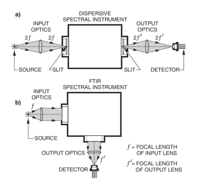
Figure 5a shows a typical optical layout of external optics relative to a dispersive monochromator. Figure 5b shows the same for an FT-IR spectrometer. The main optical feature of the FT-IR is that there are no focusing elements inside the instrument; it works with parallel beams. Dispersive instruments from the input slit to an output slit are self-contained in the sense that major spectral characteristics are not highly dependent on how the input slit is illuminated or how the light emitting from the output slit is collected. Manipulating the light with external optics adds or reduces stray light and other optical aberrations.
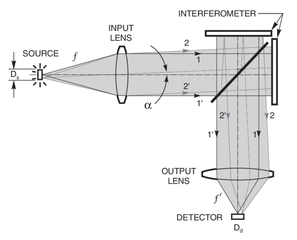
This is not the case with FT-IRs. External optics are as important for proper functioning of the instrument as their internal parts. Figure 6 shows on a larger scale a simplified scanning Michelson interferometer coupled with a source and a detector. Suppose first that the source is a (monochromatic) point source and therefore the beam entering the interferometer (rays 1-1') is perfectly parallel. Exiting the interferometer it will be focused into a point on the detector’s active area. With motion of the scanning mirror, the detector will register an interferogram - a sequence of constructive and destructive interactions between two portions of the beam in the interferometer. The further the scanning mirror is traveling, the longer the interferogram and the higher the spectral resolution that can be achieved.
In real life, point sources as well as purely parallel beams, do not exist. A finite size source produces a fan of parallel beams inside the interferometer.
A marginal beam, 2-2', of this fan is shown in Figure 6. This beam will be focused at some distance from the center of the detector. To be exact it will be focused into a ring if the source has a round shape. Now the simple picture we had before becomes much more complex since interference conditions will be different for the beams 1-1' and 2-2'.
At ZPD, both beams 1-1' and 2-2' are at constructive interference conditions and the whole detector will sense a high level of intensity. But while the scanning mirror moves away from ZPD, the next condition of constructive interference will happen sooner for beam 2-2' than for beam 1-1'. As a result, different parts of the detector will see different phases of the interference pattern: a maximum in the center will be surrounded by a ring of minimum intensity, then a ring at maximum intensity again, etc.
The farther the scanning mirror moves, the tighter this ring pattern becomes, so the detector will see an average level of intensity, and the distinct interference pattern recorded for the collimated input will be smeared. To get it back, we need to have just one fringe across the detector when the ring pattern is the tightest, in other words, when the OPD has its maximum value.
External Optics for FT-IR Instruments
General Considerations
The function of external optics for FT-IRs is not only to collect and collimate light, but also to provide a certain acceptance angle in the system according to the resolution formula:
Where:
αmax = the maximum divergence half angle (in radians)
σmax = the maximum wavenumber in the spectrum
Δσ = spectral resolution
To be able to perform calculations for FT-IR auxiliary optics we will need first to revisit some basic optical ideas.
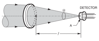
Consider light collected by a lens onto a focal spot or emitted by a source placed in the focal plane of a lens. The solid angle of the cone of rays collected from the source, or alternately directed onto the focal spot, is given by:
Ω = AL/f2 ........................................ (4)
Where:
AL = the area of the collecting/focusing lens
f = lens focal length
Both f and AL are expressed in the same units, e.g.
m, m2, or mm, mm2. We can use F/# instead of focal length,
Ω = π/(4(F/#)-2) sr ....................... (5)
So, an F/4 lens collects a solid 0.05 sr, while an F/1 lens collects 0.79 sr. In the more familiar two dimensional picture we use the divergence angle related to the solid angle by:
α2 =Ω/ π radians2 ......................... (6)
The product of solid angle and area of an image at a plane where the solid angle originates is called by various names: optical extent, geometrical extent or étendue. (Often, the term throughput is used instead of étendue.) Étendue determines the “radiation capacity” of an optical system. The fundamental law of optics states that any optical system can be characterized by an optical extent/étendue/throughput which stays constant through all optical transformations:
G = A*Ω = constant ...................... (7)
Note that in Figure 7, the area A is that of the “detector.” The relevance of this is that every optical system has something that sets or limits the value of G and it is often the detector section. Knowing what part that is and improving it as best as possible is fruitful. Working to increase the G value for another part of the system is a waste of time, but a very common waste of time.
In what follows, we consider the étendue of the MIR 8035™ FTIR Scanner. In general we start by calculating the largest étendue we can tolerate to achieve the resolution we need. If the étendue of the instrument, including source and detector, is larger than that value, then we have to limit it.
Let's determine the resolution limit on étendue for the MIR 8035™ FTIR Scanner. We know that it has an aperture of 1.25 inches (31.75 mm). We can also find a maximum allowed divergence angle of a beam propagating through it according to a maximum wavenumber in a spectrum and required resolution. From this we can find the maximum solid angle of the fan of rays by making use of equation (6). Thus, we will find the étendue of the interferometer:
Gintfr = 2.5*103*[Δσ]/[σmax]mm2 sr.................(8)
When collecting spectra with wavelengths longer than 2 µm, σmax = 5,000 cm-1, and Δσ = 0.5 cm-1,
Gintfr = 0.25 mm2 sr
Detector Optics
Now let us consider auxiliary optics; first, on the detector side. Suppose that the allowed acceptance angle is completely filled with light. Continuing the conditions cited in the example above, we want to collect this light and squeeze it onto the smallest possible detector, since smaller detectors have better noise characteristics. To do this we will take a very fast lens with F/# = 1. Then according to (5) the solid angle at the focal spot will be:
Ω = 0.79 sr
and useful detector diameter,
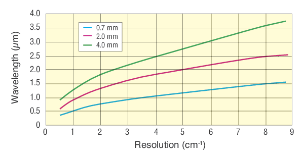
Figure 8 shows the shortest wavelength (in µm) achievable at various resolutions (in cm-1)for 3 other detector diameters (in mm). Similar relations apply to the source side. If we optimize the system for high resolution, we miss the opportunity to input a lot more radiation at lower resolutions.
What can we do in this situation? We do not have the luxury of using a different detector for each resolution. For general use, we can choose one detector which corresponds to a reasonably high, but not necessarily the highest, resolution. 4 cm-1 is a popular choice for this, because 4 cm-1 resolution is adaptable for condensed phase work. Subsequently, what if we need a higher resolution? There are a couple of ways to handle this eventuality. One way is to increase the focal length of the detector’s fore optics. Longer focus means higher F/#, lower throughput, and a higher allowed resolution. This means, of course, radiation loss also.
Another way is to use an aperture (Jacquinot Stop) to increase the F/#, by decreasing the effective source size; this reduces the spot size on the detector
Source Optics
The source with its optics will typically present a beam with étendue greater than the required étendue of the interferometer. We have seen that the étendue of the instrument is usually limited by the desired resolution or detector size.
More Considerations on Optical Elements for FT-IRs
Parabolic Mirrors
Most FTIR instruments use Off-Axis Replicated Parabolic Mirrors for collimating and focusing light external to the interferometer. These gold coated mirrors are typically broadband, from 0.7 to 10 microns, and they reflect more than 98% up to 25 microns (bear in mind that for wavelengths shorter than 0.6 micron, gold is a bad reflector; its reflectivity drops sharply to less than 40%). An important feature of mirrors in general is that they do not have any dispersion: there is no chromatic aberration so the focal spot remains the same for any wavelength in that range. They do have monochromatic aberrations.
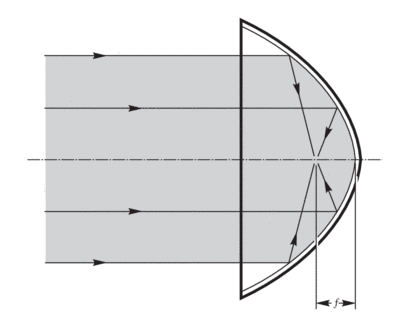
Parabolae are devices ideally suited for collimating light from small sources, and conversely, for tightly focusing collimated beams of radiation. They are, however, confined for this purpose. They cannot be used for imaging of larger objects.
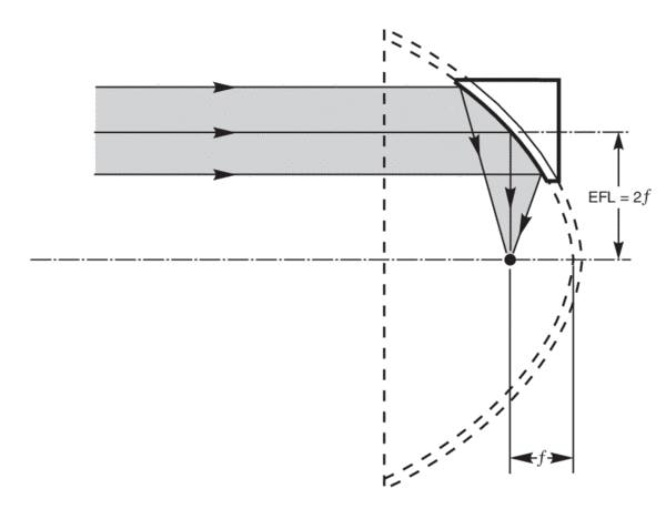
Light from a point source placed in a focus of a parabola (Figure 9) will be transformed after reflection into an ideally parallel beam. Accordingly, a parallel beam will be focused into a tiny focal spot. This is true for any section of the parabola. So, an off-axis section of the paraboloidal mirror can be cut out for convenience (see Figure 10).
The arrangement shown in Figure 10 is described as a 90° off-axis mirror since the ray striking the center of the aperture and parallel to the main axis turns exactly at 90° and comes into the focal point. The distance from the point on the surface of the parabola at the center of the aperture, to the focal point, is called the effective focal length (EFL) and it is exactly two times the focal length of the parabola.
EFL = 2f ................................ (10)
F/numbers of off-axis parabolic mirrors can reach very low values; F/1 or even less is practical. If a finite size source, instead of a point source, is placed in the focal point of the parabola, the reflected beam will not be ideally parallel. It will have some angular divergence according to the angular size of the source. On top of that, it will suffer significant aberrations. Accordingly, a parallel incoming beam will not be focused into a spot, but into a blurred spot.
It is important to analyze how the angular divergence of a beam turns into a blur spot in a parabola focus. We created the optical layout of the MIR 8035™ FTIR Scanner with an F/1 parabolic mirror at the output. The effective focal length of the mirror is 20 mm. Using an optical design software program, we traced rays with different divergence angles through the system, and observed changes to the focal spot size of the beam.
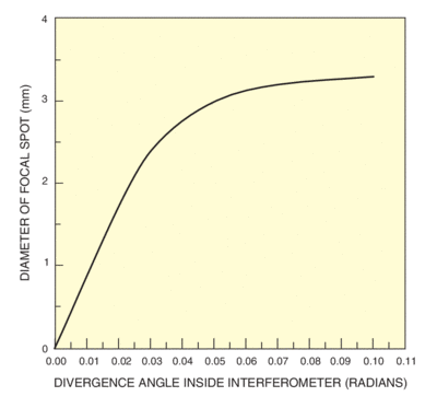
Figure 11 shows a graph of the diameter of the focal spot vs. angular divergence of the beam propagating through the interferometer.
The limit on the divergence angle in the interferometer can be found from formula (3), at the smallest possible Δσ which is 0.5 cm-1, with the highest possible σ which is 14,000 cm-1. This was found to be 0.006 rad. The graph shows that the diameter of the focal spot which corresponds to this value is about 0.5 mm. (The rough estimate, of the same value made with the formulae on the preceding pages, gives a value of 0.4 mm). With increasing divergence of the beam, the diameter of the focal spot also increases, as we see, but it has some limit between 1.5 and 2 mm. The reason for this is that the interferometer itself is blocking high angle rays and they cannot reach the parabola. The maximum value of angle of rays that can get through the interferometer is 0.06 - 0.07 rad. This is exactly the region of the curve in Figure 11 that starts to flatten out.
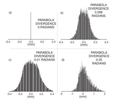
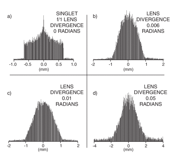
Figure 12 shows the energy distribution in the focal plane of the off axis reflector for beams of different divergence angles. This shows the increasing impact of aberrations as the “field of view” of the parabola is increased.
Lenses
Despite universality and wide usage of off-axis parabolic mirrors in FT-IR spectroscopy, they have certain disadvantages. They are relatively difficult to align as each reflection turns the beam through 90°, which can also make the system bulky. At low F/#, i.e. large fields of view (high étendue), they suffer from significant aberrations.
In many applications, especially in the Near IR, lenses could be a good choice. Figure 13 shows the energy distribution in the focal spot of a CaF2 lens having about the same focal length and F/# as the parabolic mirror considered earlier
When using Infrared Plano-Convex Lenses, we need to consider the lens material. We recommend the use of CaF2 lenses in the whole range where the CaF2 beam splitter is applicable, 14,000 – 1,200 cm-1 or 0.7 – 8.3 µm. In the very Near IR, up to 3 µm, fused silica lenses are fine, though the water absorption bands can cause some loss with lenses that are not "IR grade". They are somewhat cheaper than CaF2 lenses. A wide variety of materials are available for the Mid IR. There is usually a choice among performance, expense, durability, birefringence, etc. The hygroscopic nature of some materials can be a major problem. NaCl windows and KBr are two such materials that are commonly used. Some materials are transparent in the visible while others are not; this can be a positive if trying to align in the visible range, or a negative when the material should act as a filter.
A popular, rugged, and transparent material which is used for manufacturing lenses is ZnSe. It has, however, a very high index of refraction that pushes reflectance losses to relatively high levels: up to 30%. Anti-reflection coatings can help, but at further expense, and at a reduction of the spectral range.
A second issue is dispersion of the lens material. Lenses are definitely good for limited wavelength range applications. For example, the sensitivity range of an InGaAs detector is from 800 to 1700 nm. Using a lens should not pose a major problem, though we do see some dispersion in our labs with fused silica lenses over this range; i.e. we can axially move the lens to optimize the long wavelength or short wavelength signal. For a wider wavelength range we should position the detector at the shortest focal length position, in other words, in the position of minimum spot size for the shortest wavelength, since this is usually where the system efficiency is the lowest.
These examples show us that the auxiliary optics for an interferometer must be carefully chosen and arranged. Poor choices of components will lead to a reduction of resolution or unnecessary system throughput limitations.
