Deep UV Photolithography

DUV technology for photolithography is exclusively based on projection optics since the pattern on the photomask is much larger than the final pattern developed on the photoresist. The optical system in a 193 nm photolithography tool is known as a catadioptric system. The term means that it uses both lens (refractive) and mirror (reflective) elements for directing and conditioning the light from the laser. Details regarding the operation of such elements can be found in Mirror Physics and Optical Lens Physics. The advantage of this type of system is that it accommodates a broad bandwidth of the source laser light while limiting chromatic aberration. Refractive elements in the optical system are fabricated from either synthetic fused silica or calcium fluoride, materials that have low absorption of 193 nm light. Photomasks (or reticles) in these systems are typically made from fused silica with chrome patterns. Figure 1 shows a schematic of the exposure mechanism and relative motions of the reticle and wafer in a step-and-scan exposure system along with how water immersion is maintained between the objective lens and the wafer. In the step-and-scan process, a slit of light is scanned across one or more dies patterned on the reticle. The light reproduces the part of the pattern on the reticle that is illuminated on the wafer, albeit at much reduced feature size owing to passage through the reduction lens. Simultaneous (and highly precise, accurate, and repeatable) movement of both the reticle and the wafer is used to produce the full image of the die on the wafer. Once a die has been patterned, the process "steps" over to the next die area to be patterned.
Configuration and relative motions in a step-and-scan exposure tool
Figure 1. (a) Configuration and relative motions in a step-and-scan exposure tool; (b) water immersion arrangement (figure reprinted with permission from Lachina).
The catadioptric projection optical approach is discussed below with other semiconductor photolithography technologies described in available monographs. The physics of light are a strong determinant for the ultimate resolution (or minimum feature size) achievable in a given photolithography process (along with other factors related to substrate and resist properties and design methodologies). The smallest linewidth (W) that can be printed is determined by the wavelength (λ) of the exposing light and by the NA of the projection optics according to the Rayleigh equation:
The basic grating equation
k1 is a factor that accounts for the processing characteristics such as the quality of the resist and the use of resolution enhancement techniques like off-axis illumination. k1 has a theoretical minimum of 0.25, although values below 0.3 are considered too difficult or expensive for common use. The NA is a measure of the optical systemÕs ability to collect and focus the light from the source. Figure 2 shows the relation between the NA of a lens system and other relevant parameters in the system. In terms of smaller feature sizes, a larger NA is desirable since it reduces the minimum feature size achievable in the photolithography system. The maximum NA of a lens operating with air as the imaging medium is 1.0, although values greater than 0.95 are not normally found. Typical linewidths for single exposure patterning with λ = 193 nm immersion scanners are around 40 nm. This can be reduced with design methods and additional multiple patterning techniques to produce 22 nm feature sizes and smaller (see below).
The relationship between NA, the half-angle of the light cone, and the refractive index of the imaging medium between the lens and the substrate
Figure 2. The relationship between NA, the half-angle of the light cone, and the refractive index of the imaging medium between the lens and the substrate (reprinted with permission of Molecular Expressions.com at Florida State University).
The aim of photolithography is to produce accurate 2D images, but the optical imaging technique is inherently 3D because the aerial image is projected into air and then onto the photoresist. A consequence of this is that the expected sharp contrast between light intensity in the bright and dark areas of an image is reduced because a gradient is present in the light intensity (see Figure 3). This can reduce the quality of a lithographically-patterned line. The Normalized Image Log-Slope (NILS) method is used to quantify the aerial image quality. Minimum acceptable NILS values can be calculated using empirically-determined constants.
The NILS method used to assess image quality in photolithography
Figure 3. The NILS method used to assess image quality in photolithography.
The depth of focus (DOF) is the vertical distance over which the image remains in focus. A sufficiently high DOF is required for the entire resist layer to be developed during photolithography. The DOF is also determined by λ and NA according to:
The basic grating equation
where k2 is related to k1 and has a minimum value of 0.5 with conventional resist technologies. Using this representative value for k2 and a maximum NA of 0.95 shows that resist thicknesses are limited to about 100 nm for conventional 193 nm applications. The use of systems with higher k2 values, e.g., systems employing advanced resists such as polymethyl methacrylate and other system modifications, allows thicker resists to be used.

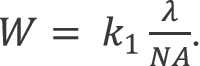
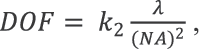
These rules highlight the key parameters that have been adjusted as photolithography technology has progressed to smaller and smaller feature sizes. The Rayleigh equation shows that, to reduce the feature size, one must either reduce the wavelength of the exposing light or increase the NA of the projection optics. The DOF must be sufficient to ensure accuracy and precision in the feature size through the entire thickness of a resist. Simplistically, the feature size that is achievable in a lithography process depends on the Rayleigh equation, while the process yield is dependent on the projection system's DOF.

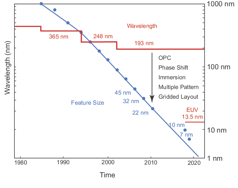
Figure 4 shows the historical progression of IC feature sizes and the wavelength of the photolithography light source required to achieve these feature sizes. Until recently, photolithography equipment designers have focused primarily on wavelength reduction to achieve smaller feature sizes:

  • Arc lamp systems developed in the 1970's and early 1980's (λ = 436 nm) are useful down to feature sizes of about 450 nm
  • Mercury lamp I-line systems developed in the mid-1980's (λ = 365 nm) are useful down to feature sizes of about 380 nm
  • KrF excimer laser-based systems developed in the 1990's (λ = 248 nm) are useful down to feature sizes of about 250 nm
  • ArF excimer laser-based systems (λ = 193 nm) are useful down to feature sizes of about 65 nm
Historical progression of IC feature size and photolithography technologies
Figure 4. Historical progression of IC feature size and photolithography technologies.
Modern DUV photolithography systems employ ArF excimer lasers at 193 nm and would be conventionally limited to feature sizes ≥ 65 nm or larger when air (NA = 1) is the medium between the optical system and the substrate. Since light sources below 193 nm were not readily available at the time (see below for EUV sources), advanced techniques were required to achieve the needed reductions in feature size for the 45, 32, and 22 nm technology nodes. By creative use of different combinations of optical proximity correction (OPC), phase shift, immersion lithography, and multiple patterning, manufacturers have extended 193 nm lithography to produce feature sizes significantly below conventional expectations. Specific details of these techniques are addressed below. Dry 193 nm photolithography in combination with double patterning has been successfully employed in 45 nm patterning technology. This technology has been adapted to include immersion lithography that has achieved 32 nm (and below) patterning technology.

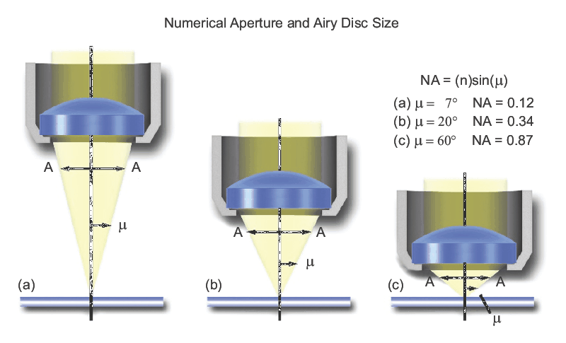
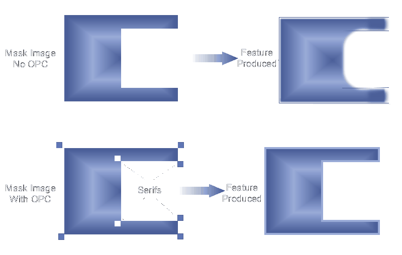
OPC techniques compensate for image distortions that occur when printing feature sizes smaller than the wavelength of the exposing light. Typically, these distortions result in shortening of line ends, corner rounding or changes to linewidths. OPC corrections are made at the mask level and involve changes to the mask image such as the addition of serifs at design corners and augmentation to linewidths. Figure 5 shows a simple example of how OPC corrections are made at the mask level.

Representative OPCs to a photomask
Figure 5. Representative OPCs to a photomask.
Phase shift is a technique that enhances edge contrast in the image being patterned, removing defects that occur due to diffraction limitations at sub-wavelength patterning. Phase shift masks do this by changing the thickness of different sections of the pattern on the mask, which changes the phase of the transmitted light passing through (Figure 6).
Shifting the phase of light by using different mask thicknesses
Figure 6. Shifting the phase of light by using different mask thicknesses.
Figure 7 depicts immersion lithography, which bypasses the feature size limitations of dry lithography by changing the medium between the optical system and the substrate from air to water. Since water has a refractive index of 1.44, this increases the value of NA beyond 1.0, leading to a reduction in minimum single-exposure feature size to about 40 nm when using 193 nm light. Water has come into standard use as the medium in immersion lithography systems since immersion techniques both increase the amount of light that can reach the resist (increasing the resolution) and change the phase of the light so that it improves DOF. For these and other reasons, single exposure immersion lithography is the dominant approach for patterning in advanced device fabrication processes at design nodes down to 45 nm.
Layout and optical characteristics of immersion lithography
Figure 7. Layout and optical characteristics of immersion lithography.
Below the 45 nm node, the combination of 193 nm immersion lithography with enhanced techniques such as multiple, i.e., double, triple, quadruple, patterning provided the smallest possible feature sizes until the advent of cost-effective EUV lithography. Quadruple patterning using multiple, shifted exposures, such as the process shown in Figure 8, effectively lowered the feature size limits. Quadruple patterning has provided a solution for patterning features as small as 5 nm.
Multiple patterning technique
Figure 8. Multiple patterning technique.

MKS Semiconductor Handbook Cover

For additional insights into photonics topics like this, download our free MKS Instruments Handbook: Principles & Applications in Photonics Technologies

Request a Handbook