Silicon Wafer Production

Create Complex Thin Films and 3D Features for Advanced Memory and Logic Nodes

Smartphones and other mobile consumer electronic devices continue to get thinner and more compact while simultaneously increasing their ability to process, consume and store large amounts of data without negatively impacting overall device battery life and end-user experience. These trends drive the need for denser transistor structures and 3D architectures for logic and memory ICs. Traditional manufacturing processes like Physical Vapor Deposition (PVD), Chemical Vapor Deposition (CVD), and Reactive Ion Etch (RIE) cannot easily produce the extremely thin films and smaller features used in advanced logic and memory technology nodes. Newer technologies like Atomic Layer Deposition (ALD) and Atomic Layer Etch (ALE) create thin films and complex 3D architectures one monolayer or atom at a time using tailored, selflimiting, cyclical chemical reactions at low temperature. The activation method is either thermal or plasma. In both ALD and ALE, a precursor adsorbs on the thin film surface forming a chemically bound monolayer. A reactant is introduced, chemically reacting with the previously modified monolayer surface, resulting in either growth or removal of a thin film layer. Byproducts from the reaction are purged and the process repeats for as many cycles as needed.

Atomic Layer Deposition Challenges

ALD creates very thin, highly tuned, conformal dielectric and metal films, barrier layers and spacers several Angstroms thick. A wide variety of precursors are used to create smooth thin films free of pinholes ensuring good electron mobility and IC functionality. These films help maximize performance characteristics of smaller features and stacked 3D architectures. Challenges specific to ALD include:

  • Precursor reactivity
  • Film uniformity
  • Achieving contamination-free layers

Atomic Layer Deposition Solutions

ALD produces the thin films needed for small, dense, and high aspect ratio (HAR) features used in complex 3D architectures. ALD, either thermal or plasma activated, uses pure metals, metal oxides, and nitrides to create highly tunable thin films for high-k/metal gates, liners in dual damascene metallization, spacers for double patterning, and dielectric and metal layers.

Ozone Generation

In thermal processing, the reaction occurs in a heated chamber, not exceeding 400°C, and is driven by wafer surface temperature and precursor concentration. O2 is the traditional precursor created by the chemical breakdown of water. Increased use of oxide compounds to create thin films requires a higher purity O2 source to reduce film contamination. MKS Ozone Generators provide high flow concentrated ozone that is ultra-pure, eliminating hydrogen and hydroxyl contamination that occurs with water. Carbon contamination is reduced by the ozone’s highly oxidizing nature. This results in very pure thin films that are very electrically efficient due to low leakage current.

Plasma Generation

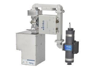
Plasma-activated atomic-level processing is an alternative when the materials being used can’t withstand the higher temperature requirements of thermal ALD. A remote plasma source or RF power generator and match network create free radicals enabling the reaction between the precursor and wafer surface at lower temperature. Radicals improve chemical reactivity with the wafer surface resulting in shorter processing times and thinner films. Remote Plasma Sources support H2 and other process chemistries. Using an enhanced plasma block for improved hydrogen radical output, and with hydrogen flow up to 5 slm, our solution provides stoichiometry control enabling tailored thin film composition.

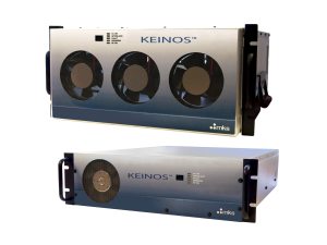
RF Plasma Generators produce the widest range of radicals including elemental metals such as Ta, Ti and Pt, and nitrides and carbides. The addition of a bias to the RF generator provides directionality to the radicals, enabling better thin film deposition of features like high aspect ratio fins and finer adjustment of film properties. This high degree of film tailoring improves future atomic layer etch results. MKS’s RF Generators have advanced pulsing capabilities that support quick switching of precursors, shortening thin film processing time and increasing throughput.

Atomic Layer Etch Challenges

ALE creates trenches and gaps, trims vertical structures like fins, and removes thin films like interfacial oxide layers at the atomic or monolayer level. Precise control over feature architecture reduces variation die-to-die and wafer-to-wafer resulting in higher yields without causing damage to the surrounding structures or the wafer. Challenges specific to ALE include:

  • Selective material removal
  • Precise etching
  • Wide range of materials
  • Low damage to surrounding features

Atomic Layer Etch Solutions

Plasma Generation

ALE provides a flat etch surface, eliminating micro-trenching that occurs with a continuous etch process. MKS RF Plasma Generators, with advanced pulsing capability, provide a level of control over plasma chemistry, separating neutrals from ions allowing saturation during the pulse off stage. The bias provides directionality to the ions further enabling anisotropic etching. These combined features enable selective, precise material removal for deep trenches and HAR features. The generated species are highly reactive and gentle, shortening processing time and reducing damage to the wafer and surrounding structures. The end results are highly repeatable critical dimensions and better IC performance. MKS RF Plasma Generators etch at low power, making them the right choice for delicate films.

Microwave Plasma Sources

To better enhance film stoichiometry in specific applications, microwave plasma sources are gaining traction. MKS’s Microwave Subsystems provide multiple power delivery frequencies that can be mixed in a process recipe to increase film stoichiometry. This results in a more reliable and efficient IC.

Atomic Layer Processing Solutions

Pressure Measurement

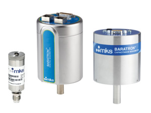
The ALD process requires high vacuum and precise pressure measurement and control to ensure the resulting monolayer film has the correct composition and uniformity. The pressure measurement device is in situ and during deposition, residual reactants can potentially cause unwanted pressure measurement drift. The unique patented technology of MKS Baratron® Capacitance Manometers minimizes residual deposition and ensures low pressure measurement drift, resulting in highly reproducible thin films. To avoid condensation build-up, the capacitance manometer is heated making it thermally compatible and, using the EtherCAT® protocol, it communicates rapidly with the overall system, improving speed of response.

Pressure Control

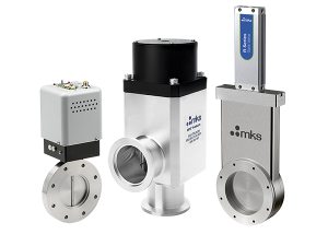
Controlling gas volume improves process efficiency and reduces the cost of expensive precursors. MKS Pressure Controllers, positioned at the inlet of the chamber, provide precise precursor delivery control by sending a highly concentrated volume of gas to the chamber and stopping gas flow quickly once volume is achieved. MKS High Speed Throttle Valves, located at the outlet, build pressure quickly inside the chamber using a unique, soft-sealing technology and rapidly modulate pressure caused by the influx of gas with fast opening and closing valve operation. Precise control of gas flow and chamber pressure reduces the amount of wasted gas and ensures optimum chemical reactivity resulting in good thin film deposition.

Thermal Management

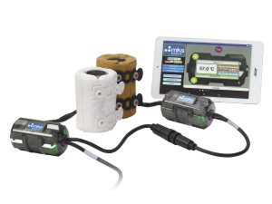
Temperature differences between feed lines and the process chamber can lead to condensation of precursor gas causing variation in delivered gas volume. This leads to insufficient precursor gas for the chemical reaction resulting in incomplete deposition or etch. The MKS Thermal Management System consists of advanced heater jackets made with highly energy-efficient materials, a controller with customized temperature operation, and an intuitive user interface that allows accurate and precise temperature control. This guarantees a selfsaturating, self-limiting reaction resulting in high quality, uniform film deposition and precise etching of complex structures. Similarly, the MKS Thermal Management System can be utilized for effective pumpline temperature management.

Semiconductor Devices and Process Technology Handbook

For additional information on the semiconductor atomic layer processing as well as other semiconductor applications please download our free Semiconductor Devices and Process Technology eBook.

Atomic Layer Processing Products